- 您现在的位置:买卖IC网 > PDF目录79699 > LT1375IN8#TRPBF (LINEAR TECHNOLOGY CORP) 3 A SWITCHING REGULATOR, 570 kHz SWITCHING FREQ-MAX, PDIP8 PDF资料下载
参数资料
| 型号: | LT1375IN8#TRPBF |
| 厂商: | LINEAR TECHNOLOGY CORP |
| 元件分类: | 稳压器 |
| 英文描述: | 3 A SWITCHING REGULATOR, 570 kHz SWITCHING FREQ-MAX, PDIP8 |
| 封装: | 0.300 INCH, LEAD FREE, PLASTIC, DIP-8 |
| 文件页数: | 23/28页 |
| 文件大小: | 500K |
| 代理商: | LT1375IN8#TRPBF |
第1页第2页第3页第4页第5页第6页第7页第8页第9页第10页第11页第12页第13页第14页第15页第16页第17页第18页第19页第20页第21页第22页当前第23页第24页第25页第26页第27页第28页
4
LT1375/LT1376
13756fd
ELECTRICAL CHARACTERISTICS
Note 1: Stresses beyond those listed under Absolute Maximum Ratings
may cause permanent damage to the device. Exposure to any Absolute
Maximum Rating condition for extended periods may affect device
reliability and lifetime.
Note 2: Gain is measured with a VC swing equal to 200mV above the low
clamp level to 200mV below the upper clamp level.
Note 3: Minimum input voltage is not measured directly, but is guaranteed
by other tests. It is defined as the voltage where internal bias lines are still
regulated so that the reference voltage and oscillator frequency remain
constant. Actual minimum input voltage to maintain a regulated output will
depend on output voltage and load current. See Applications Information.
Note 4: This is the minimum voltage across the boost capacitor needed to
guarantee full saturation of the internal power switch.
Note 5: Boost current is the current flowing into the BOOST pin with the
pin held 5V above input voltage. It flows only during switch-on time.
Note 6: Input supply current is the bias current drawn by the input pin
when the BIAS pin is held at 5V with switching disabled. Output supply
current is the current drawn by the BIAS pin when the bias pin is held at
5V. Total input referred supply current is calculated by summing input
supply current (ISI) with a fraction of output supply current (ISO):
ITOT = ISI + (ISO)(VOUT/VIN)(1.15)
With VIN = 15V, VOUT = 5V, ISI = 0.9mA, ISO = 3.6mA, ITOT = 2.28mA.
For the LT1375, quiescent current is equal to:
ITOT = ISI + ISO(1.15)
because the BIAS pin is internally connected to VIN.
For LT1375 or BIAS open circuit, input supply current is the sum of input
+ output supply currents.
Note 7: Switch-on resistance is calculated by dividing VIN to VSW voltage
by the forced current (1.5A). See Typical Performance Characteristics for
the graph of switch voltage at other currents.
Note 8: Transconductance and voltage gain refer to the internal amplifier
exclusive of the voltage divider. To calculate gain and transconductance
refer to sense pin on fixed voltage parts. Divide values shown by the ratio
VOUT/2.42.
The
● denotes specifications which apply over the full operating
temperature range, otherwise specifications are at TA = 25°C. TJ = 25°C, VIN = 15V, VC = 1.5V, boost open, switch open,
unless otherwise noted.
PARAMETER
CONDITIONS
MIN
TYP
MAX
UNITS
Shutdown Thresholds
VC Open
Device Shutting Down
●
0.15
0.37
0.60
V
Device Starting Up
●
0.25
0.45
0.60
V
VC Open
LT1375HV/LT1376HV Device Shutting Down
●
0.15
0.37
0.70
V
LT1375HV/LT1376HV Device Starting Up
●
0.25
0.45
0.70
V
Minimum Synchronizing Amplitude (LT1375 Only)
VIN = 5V
●
1.5
2.2
V
Synchronizing Range (LT1375 Only)
580
900
kHz
SYNC Pin Input Resistance
40
k
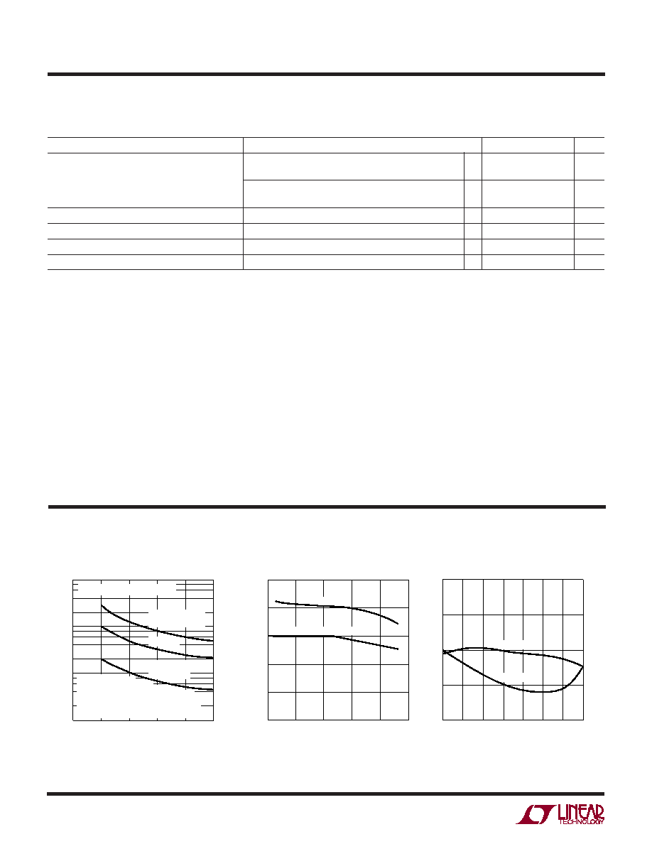
INDUCTANCE (
H)
05
CORE
LOSS
(W)
CORE
LOSS
(%
OF
5W
LOAD)
1.0
0.1
0.01
0.001
10
15
20
12
8
4
2
1.2
0.8
0.4
0.2
0.12
0.08
0.04
0.02
25
1375/76 G01
TYPE 52
POWDERED IRON
Kool M
PERMALLOY
= 125
VOUT = 5V, VIN = 10V, IOUT = 1A
CORE LOSS IS
INDEPENDENT OF LOAD
CURRENT UNTIL LOAD CURRENT FALLS
LOW ENOUGH FOR CIRCUIT TO GO INTO
DISCONTINUOUS MODE
Inductor Core Loss
TYPICAL PERFORMANCE CHARACTERISTICS
UW
DUTY CYCLE (%)
0
SWITCH
PEAK
CURRENT
(A)
2.5
2.0
1.5
1.0
0.5
0
80
1375/76 G08
20
40
60
100
TYPICAL
GUARANTEED MINIMUM
Switch Peak Current Limit
JUNCTION TEMPERATURE (
°C)
–50
2.44
2.43
2.42
2.41
2.40
100
1375/76 G09
–25
0
25
50
75
125
FEEDBACK
VOLTAGE
(V)
CURRENT
(
A)
2.0
1.5
1.0
0.5
0
VOLTAGE
CURRENT
Feedback Pin Voltage and Current
相关PDF资料 |
PDF描述 |
|---|---|
| LM4041C12IDBZRG4 | 1-OUTPUT TWO TERM VOLTAGE REFERENCE, 1.225 V, PDSO3 |
| LM4041C12QDBZRG4 | 1-OUTPUT TWO TERM VOLTAGE REFERENCE, 1.225 V, PDSO3 |
| LM4041D12QDBZT | 1-OUTPUT TWO TERM VOLTAGE REFERENCE, 1.225 V, PDSO3 |
| LM4040A25IDCKRE4 | 1-OUTPUT TWO TERM VOLTAGE REFERENCE, 2.5 V, PDSO5 |
| LTC1435AACG | SWITCHING CONTROLLER, PDSO16 |
相关代理商/技术参数 |
参数描述 |
|---|---|
| LT1375IS8 | 功能描述:IC REG BUCK ADJ 1.5A 8SOIC RoHS:否 类别:集成电路 (IC) >> PMIC - 稳压器 - DC DC 开关稳压器 系列:- 设计资源:Design Support Tool 标准包装:1 系列:- 类型:升压(升压) 输出类型:固定 输出数:1 输出电压:3V 输入电压:0.75 V ~ 2 V PWM 型:- 频率 - 开关:- 电流 - 输出:100mA 同步整流器:是 工作温度:-40°C ~ 85°C 安装类型:表面贴装 封装/外壳:SOT-23-5 细型,TSOT-23-5 包装:剪切带 (CT) 供应商设备封装:TSOT-23-5 其它名称:AS1323-BTTT-30CT |
| LT1375IS8#PBF | 功能描述:IC REG BUCK ADJ 1.5A 8SOIC RoHS:是 类别:集成电路 (IC) >> PMIC - 稳压器 - DC DC 开关稳压器 系列:- 标准包装:250 系列:- 类型:降压(降压) 输出类型:固定 输出数:1 输出电压:1.2V 输入电压:2.05 V ~ 6 V PWM 型:电压模式 频率 - 开关:2MHz 电流 - 输出:500mA 同步整流器:是 工作温度:-40°C ~ 85°C 安装类型:表面贴装 封装/外壳:6-UFDFN 包装:带卷 (TR) 供应商设备封装:6-SON(1.45x1) 产品目录页面:1032 (CN2011-ZH PDF) 其它名称:296-25628-2 |
| LT1375IS8#PBF | 制造商:Linear Technology 功能描述:ICSMPS CONTROLLERCURRENT-MOD 制造商:Linear Technology 功能描述:IC,SMPS CONTROLLER,CURRENT-MODE,BIPOLAR, |
| LT1375IS8#TR | 功能描述:IC REG BUCK ADJ 1.5A 8SOIC RoHS:否 类别:集成电路 (IC) >> PMIC - 稳压器 - DC DC 开关稳压器 系列:- 标准包装:2,500 系列:- 类型:降压(降压) 输出类型:固定 输出数:1 输出电压:1.2V,1.5V,1.8V,2.5V 输入电压:2.7 V ~ 20 V PWM 型:- 频率 - 开关:- 电流 - 输出:50mA 同步整流器:是 工作温度:-40°C ~ 125°C 安装类型:表面贴装 封装/外壳:10-TFSOP,10-MSOP(0.118",3.00mm 宽)裸露焊盘 包装:带卷 (TR) 供应商设备封装:10-MSOP 裸露焊盘 |
| LT1375IS8#TRPBF | 功能描述:IC REG BUCK ADJ 1.5A 8SOIC RoHS:是 类别:集成电路 (IC) >> PMIC - 稳压器 - DC DC 开关稳压器 系列:- 标准包装:2,500 系列:- 类型:降压(降压) 输出类型:固定 输出数:1 输出电压:1.2V,1.5V,1.8V,2.5V 输入电压:2.7 V ~ 20 V PWM 型:- 频率 - 开关:- 电流 - 输出:50mA 同步整流器:是 工作温度:-40°C ~ 125°C 安装类型:表面贴装 封装/外壳:10-TFSOP,10-MSOP(0.118",3.00mm 宽)裸露焊盘 包装:带卷 (TR) 供应商设备封装:10-MSOP 裸露焊盘 |
发布紧急采购,3分钟左右您将得到回复。