- 您现在的位置:买卖IC网 > PDF目录10685 > LT1394IS8#TR (Linear Technology)IC COMPARATOR 7NS LOW PWR 8SOIC PDF资料下载
参数资料
| 型号: | LT1394IS8#TR |
| 厂商: | Linear Technology |
| 文件页数: | 14/16页 |
| 文件大小: | 0K |
| 描述: | IC COMPARATOR 7NS LOW PWR 8SOIC |
| 标准包装: | 2,500 |
| 系列: | UltraFast™ |
| 类型: | 带锁销 |
| 元件数: | 1 |
| 输出类型: | CMOS,补充型,TTL |
| 电压 - 输入偏移(最小值): | 2.5mV @ ±5V |
| 电流 - 输入偏压(最小值): | 4.5µA @ ±5V |
| 电流 - 输出(标准): | 20mA |
| 电流 - 静态(最大值): | 8.5mA |
| CMRR, PSRR(标准): | 100dB CMRR,100dB PSRR |
| 传输延迟(最大): | 9ns |
| 工作温度: | -40°C ~ 85°C |
| 封装/外壳: | 8-SOIC(0.154",3.90mm 宽) |
| 安装类型: | 表面贴装 |
| 包装: | 带卷 (TR) |
7
LT1394
APPLICATIONS INFORMATION
WU
U
Common Mode Considerations
The LT1394 is specified for a common mode range of – 5V
to 3.5V on a
±5V supply or a common mode range of 0V
to 3.5V on a single 5V supply. A more general consider-
ation is that the common mode range is 0V below the
negative supply and 1.5V below the positive supply, inde-
pendent of the actual supply voltage. The criterion for
common mode limit is that the output still responds
correctly to a small differential input signal.
When either input signal falls below the negative common
mode limit, the internal PN diode formed with the sub-
strate can turn on, resulting in significant current flow
through the die. An external Schottky clamp diode
between the input and the negative rail can speed up
recovery from negative overdrive by preventing the sub-
strate diode from turning on. The zero-crossing detector
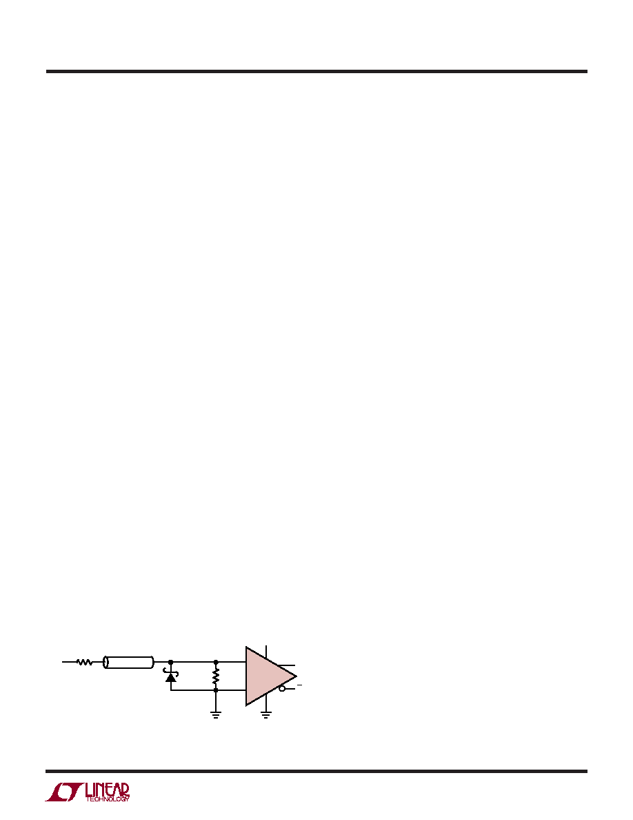
in Figure 1 demonstrates the use of a fast clamp diode.
The zero-crossing detector terminates the transmission
line at its 50
characteristic impedance. Negative inputs
should not fall below – 2V to keep the signal current within
the clamp diode’s maximum forward rating. Positive
inputs should not exceed the device’s absolute maximum
ratings or the power rating on the terminating resistor.
Either input may go above the positive common mode
limit without damaging the comparator. The upper voltage
limit is determined by an internal diode from each input to
the positive supply. The input may go above the positive
supply as long as it does not go far enough above it to
conduct more than 10mA. Functionality will continue if the
remaining input stays within the allowed common mode
range. There will, however, be an increase in propagation
delay as the input signal switches back into the common
mode range.
Figure 1. Fast Zero-Crossing Detector
Input Bias Current
Input bias current is measured with the output held at
1.4V. As with any PNP differential input stage, the LT1394
bias current flows out of the device. It will go to zero on an
input which is high and double on an input which is low.
LATCH Pin Dynamics
The LATCH pin is intended to retain input data (output
latched) when the LATCH pin goes high. The pin will float
to a high state when disconnected, so a flow-through
condition requires that the LATCH pin be grounded. The
LATCH pin is designed to be driven with either a TTL or
CMOS output. It has no built-in hysteresis.
To guarantee data retention, the input signal must remain
valid at least 2ns after the latch goes high (hold time), and
must be valid at least – 0.4ns before the latch goes high
(setup time). The negative setup time simply means that
the data arriving 0.4ns after (rather than before) the latch
signal is valid. When the latch signal goes low, new data
will appear at the output in approximately 6ns (latch
propagation delay).
Measuring Response Time
To properly measure the response of the LT1394 requires
an input signal source with very fast rise times and
exceptionally clean settling characteristics. The last
requirement comes about because the standard compara-
tor test calls for an input step size that is large compared
to the overdrive amplitude. Typical test conditions are
100mV step size with 5mV overdrive. This requires an
input signal that settles to within 1% (1mV) of final value
in only a few nanoseconds with no ringing or settling tail.
Ordinary high speed pulse generators are not capable of
generating such a signal, and in any case, no ordinary
oscilloscope is capable of displaying the waveform to
check its fidelity. Some means must be used to inherently
generate a fast, clean edge with known final value. The
circuit shown in Figure 2 is the best electronic means of
generating a fast, clean step to test comparators. It uses
a very fast transistor in a common base configuration. The
transistor is switched off with a fast edge from the genera-
tor and the collector voltage settles to exactly 0V in just a
few nanoseconds. The most important feature of this
1394 F01
5V
–
+
LT1394
Q
CABLE
RT
50
VIN
RS
50
1N5712
相关PDF资料 |
PDF描述 |
|---|---|
| LT1394CMS8#TRPBF | IC COMPARATOR 7NS LOW PWR 8MSOP |
| LT1394CMS8#TR | IC COMPARATOR 7NS LOW PWR 8MSOP |
| VE-2NR-MY-B1 | CONVERTER MOD DC/DC 7.5V 50W |
| VI-BWJ-MY-B1 | CONVERTER MOD DC/DC 36V 50W |
| VE-2NJ-MY-B1 | CONVERTER MOD DC/DC 36V 50W |
相关代理商/技术参数 |
参数描述 |
|---|---|
| LT1395 | 制造商:LINER 制造商全称:Linear Technology 功能描述:Single/Dual/Quad 400MHz Current Feedback Amplifier |
| LT1395_1 | 制造商:LINER 制造商全称:Linear Technology 功能描述:Single/Dual/Quad 400MHz Current Feedback Amplifier |
| LT1395CS5 | 制造商:Linear Technology 功能描述:OP Amp Single Current Fdbk ±6V/12V 5-Pin TSOT-23 |
| LT1395CS5#PBF | 制造商:Linear Technology 功能描述:OP-AMP, 400MHZ, 800V/us, TSOT-23-5; Op Amp Type:Current Feedback; No. of Amplifiers:1; Slew Rate:800V/s; Supply Voltage Range:4V to 12V; Amplifier Case Style:TSOT-23; No. of Pins:5; Bandwidth:400MHz; Operating Temperature Min:0C ;RoHS Compliant: Yes |
| LT1395CS5#TR | 功能描述:IC AMP CURR FEEDBK SNGL TSOT23-5 RoHS:否 类别:集成电路 (IC) >> Linear - Amplifiers - Instrumentation 系列:- 标准包装:160 系列:- 放大器类型:通用 电路数:4 输出类型:满摆幅 转换速率:10 V/µs 增益带宽积:9MHz -3db带宽:- 电流 - 输入偏压:1pA 电压 - 输入偏移:250µV 电流 - 电源:730µA 电流 - 输出 / 通道:28mA 电压 - 电源,单路/双路(±):2.7 V ~ 5.5 V,±1.35 V ~ 2.75 V 工作温度:-40°C ~ 125°C 安装类型:表面贴装 封装/外壳:16-SOIC(0.154",3.90mm 宽) 供应商设备封装:16-SOIC N 包装:管件 |
发布紧急采购,3分钟左右您将得到回复。