参数资料
| 型号: | LT1396CDD#TR |
| 厂商: | Linear Technology |
| 文件页数: | 16/20页 |
| 文件大小: | 0K |
| 描述: | IC AMP CUR FDBK DUAL 400MHZ 8DFN |
| 标准包装: | 2,500 |
| 放大器类型: | 电流反馈 |
| 电路数: | 2 |
| 转换速率: | 800 V/µs |
| -3db带宽: | 400MHz |
| 电流 - 输入偏压: | 10µA |
| 电压 - 输入偏移: | 1000µV |
| 电流 - 电源: | 4.6mA |
| 电流 - 输出 / 通道: | 80mA |
| 电压 - 电源,单路/双路(±): | 4 V ~ 12 V,±2 V ~ 6 V |
| 工作温度: | 0°C ~ 70°C |
| 安装类型: | 表面贴装 |
| 封装/外壳: | 8-WFDFN 裸露焊盘 |
| 供应商设备封装: | 8-DFN-EP(3x3) |
| 包装: | 带卷 (TR) |
LT1395/LT1396/LT1397
5
139567fd
ELECTRICAL CHARACTERISTICS
Note 1: Stresses beyond those listed under Absolute Maximum Ratings
may cause permanent damage to the device. Exposure to any Absolute
Maximum Rating condition for extended periods may affect device
reliability and lifetime.
Note 2: This parameter is guaranteed to meet specied performance
through design and characterization. It has not been tested.
Note 3: A heat sink may be required depending on the power supply
voltage and how many ampliers have their outputs short circuited.
The
θJA specied for the DD package is with minimal PCB heat spreading
metal. Using expanded metal area on all layers of a board reduces
this value.
Note 4: The LT1395C/LT1396C/LT1397C are guaranteed functional over the
operating temperature range of –40°C to 85°C. The LT1397H is guaranteed
functional over the operating temperature range of –40°C to 125°C.
Note 5: The LT1395C/LT1396C/LT1397C are guaranteed to meet specied
performance from 0°C to 70°C. The LT1395C/LT1396C/LT1397C are
designed, characterized and expected to meet specied performance from
–40°C and 85°C but are not tested or QA sampled at these temperatures.
The LT1397H is guaranteed to meet specied performance from –40°C to
125°C. For guaranteed I-grade parts, consult the factory.
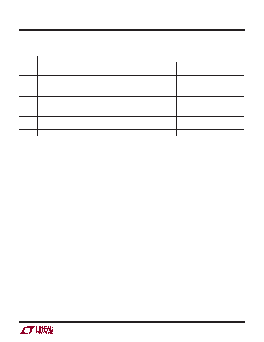
SYMBOL
PARAMETER
CONDITIONS
MIN
TYP
MAX
UNITS
tON
Turn-On Delay Time (Note 9)
RF = RG = 255Ω, RL = 100Ω, (LT1395CS6 only)
30
75
ns
tOFF
Turn-Off Delay Time (Note 9)
RF = RG = 255Ω, RL = 100Ω, (LT1395CS6 only)
40
100
ns
–3dB BW
–3dB Bandwidth
AV = 1, RF = 374Ω, RL = 100Ω
AV = 2, RF = RG = 255Ω, RL = 100Ω
400
350
MHz
0.1dB BW
0.1dB Bandwidth
AV = 1, RF = 374Ω, RL = 100Ω
AV = 2, RF = RG = 255Ω, RL = 100Ω
100
MHz
tr, tf
Small-Signal Rise and Fall Time
RF = RG = 255Ω, RL = 100Ω, VOUT = 1VP-P
1.3
ns
tPD
Propagation Delay
RF = RG = 255Ω, RL = 100Ω, VOUT = 1VP-P
2.5
ns
os
Small-Signal Overshoot
RF = RG = 255Ω, RL = 100Ω, VOUT = 1VP-P
10
%
tS
Settling Time
0.1%, AV = –1, RF = RG = 280Ω, RL = 150Ω
25
ns
dG
Differential Gain (Note 8)
RF = RG = 255Ω, RL = 150Ω
0.02
%
dP
Differential Phase (Note 8)
RF = RG = 255Ω, RL = 150Ω
0.04
DEG
Note 6:
TJ is calculated from the ambient temperature TA and the power
dissipation PD according to the following formula:
LT1395CS5: TJ = TA + (PD 250°C/W)
LT1396CS6: TJ = TA + (PD 230°C/W)
LT1395CS8: TJ = TA + (PD 150°C/W)
LT1396CS8: TJ = TA + (PD 150°C/W)
LT1396CMS8: TJ = TA + (PD 250°C/W)
LT1396CDD: TJ = TA + (PD 160°C/W)
LT1397CS14: TJ = TA + (PD 100°C/W)
LT1397CGN16: TJ = TA + (PD 135°C/W)
LT1397CDE: TJ = TA + (PD 43°C/W)
LT1397HDE: TJ = TA + (PD 43°C/W)
Note 7: Slew rate is measured at ±2V on a ±3V output signal.
Note 8: Differential gain and phase are measured using a Tektronix
TSG120YC/NTSC signal generator and a Tektronix 1780R Video
Measurement Set. The resolution of this equipment is 0.1% and 0.1°.
Ten identical amplier stages were cascaded giving an effective resolution
of 0.01% and 0.01°.
Note 9: For LT1395CS6, turn-on delay time (tON) is measured from control
input to appearance of 1V(50%) at the output, for VIN = 1V and AV = 2.
Likewise, turn-off delay time (tOFF) is measured from control input to
appearance of 1V(50%) on the output for VIN = 1V and AV = 2.
This specication is guaranteed by design and characterization.
The ● denotes specications which apply over the specied operating temperature range, otherwise specications are at TA = 25°C.
For each amplier: VCM = 0V, VS = ±5V, pulse tested, unless otherwise noted. (Note 5)
相关PDF资料 |
PDF描述 |
|---|---|
| 0878341619 | CONN HDR W/PG/SLT 16POS |
| NPPN111BFCN-RC | CONN RECEPT 2MM SINGLE STR 11POS |
| LT1783IS6#TRPBF | IC OPAMP R-R IN/OUT SOT23-6 |
| NPPN081BFCN-RC | CONN RECEPT 2MM SINGLE STR 8POS |
| NPPN051BFLD-RC | CONN RECEPT 2MM SINGLE SMD 5POS |
相关代理商/技术参数 |
参数描述 |
|---|---|
| LT1396CDD-TRPBF | 制造商:LINER 制造商全称:Linear Technology 功能描述:Single/Dual/Quad 400MHz Current Feedback Amplifier |
| LT1396CMS8 | 功能描述:IC AMP CURR FEEDBACK DUAL 8MSOP RoHS:否 类别:集成电路 (IC) >> Linear - Amplifiers - Instrumentation 系列:- 标准包装:1,000 系列:- 放大器类型:电压反馈 电路数:4 输出类型:满摆幅 转换速率:33 V/µs 增益带宽积:20MHz -3db带宽:30MHz 电流 - 输入偏压:2nA 电压 - 输入偏移:3000µV 电流 - 电源:2.5mA 电流 - 输出 / 通道:30mA 电压 - 电源,单路/双路(±):4.5 V ~ 16.5 V,±2.25 V ~ 8.25 V 工作温度:-40°C ~ 85°C 安装类型:表面贴装 封装/外壳:14-SOIC(0.154",3.90mm 宽) 供应商设备封装:14-SOIC 包装:带卷 (TR) |
| LT1396CMS8#PBF | 功能描述:IC AMP CURR FEEDBACK DUAL 8MSOP RoHS:是 类别:集成电路 (IC) >> Linear - Amplifiers - Instrumentation 系列:- 标准包装:1,000 系列:- 放大器类型:电压反馈 电路数:4 输出类型:满摆幅 转换速率:33 V/µs 增益带宽积:20MHz -3db带宽:30MHz 电流 - 输入偏压:2nA 电压 - 输入偏移:3000µV 电流 - 电源:2.5mA 电流 - 输出 / 通道:30mA 电压 - 电源,单路/双路(±):4.5 V ~ 16.5 V,±2.25 V ~ 8.25 V 工作温度:-40°C ~ 85°C 安装类型:表面贴装 封装/外壳:14-SOIC(0.154",3.90mm 宽) 供应商设备封装:14-SOIC 包装:带卷 (TR) |
| LT1396CMS8#TR | 功能描述:IC AMP CURR FEEDBACK DUAL 8MSOP RoHS:否 类别:集成电路 (IC) >> Linear - Amplifiers - Instrumentation 系列:- 标准包装:1,000 系列:- 放大器类型:电压反馈 电路数:4 输出类型:满摆幅 转换速率:33 V/µs 增益带宽积:20MHz -3db带宽:30MHz 电流 - 输入偏压:2nA 电压 - 输入偏移:3000µV 电流 - 电源:2.5mA 电流 - 输出 / 通道:30mA 电压 - 电源,单路/双路(±):4.5 V ~ 16.5 V,±2.25 V ~ 8.25 V 工作温度:-40°C ~ 85°C 安装类型:表面贴装 封装/外壳:14-SOIC(0.154",3.90mm 宽) 供应商设备封装:14-SOIC 包装:带卷 (TR) |
| LT1396CMS8#TRPBF | 功能描述:IC AMP CURR FEEDBACK DUAL 8MSOP RoHS:是 类别:集成电路 (IC) >> Linear - Amplifiers - Instrumentation 系列:- 标准包装:1,000 系列:- 放大器类型:电压反馈 电路数:4 输出类型:满摆幅 转换速率:33 V/µs 增益带宽积:20MHz -3db带宽:30MHz 电流 - 输入偏压:2nA 电压 - 输入偏移:3000µV 电流 - 电源:2.5mA 电流 - 输出 / 通道:30mA 电压 - 电源,单路/双路(±):4.5 V ~ 16.5 V,±2.25 V ~ 8.25 V 工作温度:-40°C ~ 85°C 安装类型:表面贴装 封装/外壳:14-SOIC(0.154",3.90mm 宽) 供应商设备封装:14-SOIC 包装:带卷 (TR) |
发布紧急采购,3分钟左右您将得到回复。