- 您现在的位置:买卖IC网 > PDF目录5376 > LT1397CDE#PBF (Linear Technology)IC AMP CURR FEEDBACK QUAD 14-DFN PDF资料下载
参数资料
| 型号: | LT1397CDE#PBF |
| 厂商: | Linear Technology |
| 文件页数: | 2/20页 |
| 文件大小: | 0K |
| 描述: | IC AMP CURR FEEDBACK QUAD 14-DFN |
| 标准包装: | 91 |
| 放大器类型: | 电流反馈 |
| 电路数: | 4 |
| 转换速率: | 800 V/µs |
| -3db带宽: | 400MHz |
| 电流 - 输入偏压: | 10µA |
| 电压 - 输入偏移: | 1000µV |
| 电流 - 电源: | 4.6mA |
| 电流 - 输出 / 通道: | 80mA |
| 电压 - 电源,单路/双路(±): | 4 V ~ 12 V,±2 V ~ 6 V |
| 工作温度: | 0°C ~ 70°C |
| 安装类型: | 表面贴装 |
| 封装/外壳: | 14-WFDFN 裸露焊盘 |
| 供应商设备封装: | 14-DFN-EP(4x3) |
| 包装: | 管件 |
LT1395/LT1396/LT1397
10
139567fd
Feedback Resistor Selection
The small-signal bandwidth of the LT1395/LT1396/LT1397
is set by the external feedback resistors and the inter-
nal junction capacitors. As a result, the bandwidth is a
function of the supply voltage, the value of the feedback
resistor, the closed-loop gain and the load resistor. The
LT1395/LT1396/LT1397 have been optimized for ± 5V
supply operation and have a –3dB bandwidth of 400MHz
at a gain of 1 and 350MHz at a gain of 2. Please refer to
the resistor selection guide in the Typical AC Perfor-
mance table.
Capacitance on the Inverting Input
Current feedback ampliers require resistive feedback from
the output to the inverting input for stable operation. Take
care to minimize the stray capacitance between the output
and the inverting input. Capacitance on the inverting input
to ground will cause peaking in the frequency response
(and overshoot in the transient response).
Capacitive Loads
The LT1395/LT1396/LT1397 can drive many capacitive
loads directly when the proper value of feedback resistor
is used. The required value for the feedback resistor will
increase as load capacitance increases and as closed-
loop gain decreases. Alternatively, a small resistor (5Ω
to 35Ω) can be put in series with the output to isolate the
capacitive load from the amplier output. This has the
advantage that the amplier bandwidth is only reduced
when the capacitive load is present. The disadvantage is
that the gain is a function of the load resistance. See the
Typical Performance Characteristics curves.
Power Supplies
The LT1395/LT1396/LT1397 will operate from single or split
supplies from ± 2V (4V total) to ±6V (12V total). It is not
necessary to use equal value split supplies, however the
offset voltage and inverting input bias current will change.
The offset voltage changes about 2.5mV per volt of supply
mismatch. The inverting bias current will typically change
about 10μA per volt of supply mismatch.
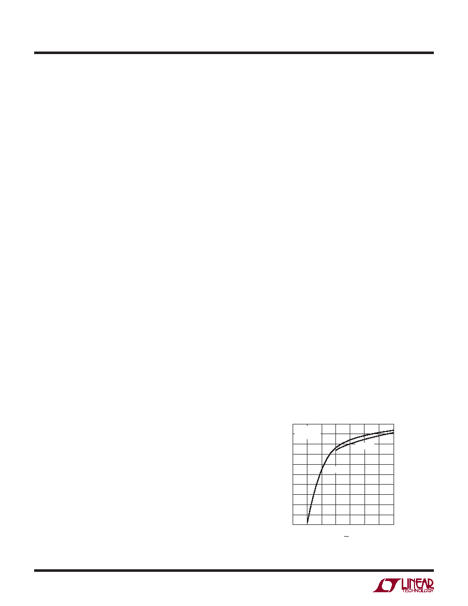
APPLICATIONS INFORMATION
Figure 1. + IS vs (V+ – VEN)
V+ – VEN (V)
0
+I
S
(mA)
0.5
1.5
2.0
2.5
5.0
3.5
2
4
5
1395/6/7 F01
1.0
4.0
4.5
3.0
1
3
6
7
TA = 25°C
V+ = 5V
V– = –5V
V– = 0V
Slew Rate
Unlike a traditional voltage feedback op amp, the slew rate
of a current feedback amplier is not independent of the
amplier gain conguration. In a current feedback ampli-
er, both the input stage and the output stage have slew
rate limitations. In the inverting mode, and for gains of 2
or more in the noninverting mode, the signal amplitude
between the input pins is small and the overall slew rate
is that of the output stage. For gains less than 2 in the
noninverting mode, the overall slew rate is limited by the
input stage.
The input slew rate of the LT1395/LT1396/LT1397 is ap-
proximately 600V/μs and is set by internal currents and
capacitances. The output slew rate is set by the value of
the feedback resistor and internal capacitance. At a gain
of 2 with 255Ω feedback and gain resistors and ± 5V
supplies, the output slew rate is typically 800V/μs. Larger
feedback resistors will reduce the slew rate as will lower
supply voltages.
Enable/Disable
The LT1395CS6 has a unique high impedance, zero sup-
ply current mode which is controlled by the EN pin. The
LT1395CS6 is designed to operate with CMOS logic; it
draws virtually zero current when the EN pin is high. To
activate the amplier, its EN pin is normally pulled to a
logic low. However, supply current will vary as the volt-
age between the V + supply and EN is varied. As seen
in Figure 1, +IS does vary with (V+ – VEN), particularly
when the voltage difference is less than 3V. For normal
相关PDF资料 |
PDF描述 |
|---|---|
| M14-4R/SX-BOTTLE | CONN RING NON-INSUL #4 100PC |
| 1SMC9.0AT3 | TVS 1500W 9.0V UNIDIRECT SMC |
| M14-10R/LX-BOTTLE | CONN RING NON-INSUL 100PC |
| 7100.1161.96 | FUSE 400MA 250V FAST 19MM PCB TR |
| 7100.1160.96 | FUSE 315MA 250V FAST 19MM PCB TR |
相关代理商/技术参数 |
参数描述 |
|---|---|
| LT1397CDE-TR | 制造商:LINER 制造商全称:Linear Technology 功能描述:Single/Dual/Quad 400MHz Current Feedback Amplifier |
| LT1397CDE-TRPBF | 制造商:LINER 制造商全称:Linear Technology 功能描述:Single/Dual/Quad 400MHz Current Feedback Amplifier |
| LT1397CGN | 功能描述:IC AMP CURR FEEDBACK QUAD 16SSOP RoHS:否 类别:集成电路 (IC) >> Linear - Amplifiers - Instrumentation 系列:- 标准包装:50 系列:- 放大器类型:通用 电路数:2 输出类型:满摆幅 转换速率:1.8 V/µs 增益带宽积:6.5MHz -3db带宽:4.5MHz 电流 - 输入偏压:5nA 电压 - 输入偏移:100µV 电流 - 电源:65µA 电流 - 输出 / 通道:35mA 电压 - 电源,单路/双路(±):1.8 V ~ 5.25 V,±0.9 V ~ 2.625 V 工作温度:-40°C ~ 85°C 安装类型:表面贴装 封装/外壳:10-TFSOP,10-MSOP(0.118",3.00mm 宽) 供应商设备封装:10-MSOP 包装:管件 |
| LT1397CGN#PBF | 功能描述:IC AMP CURR FEEDBACK QUAD 16SSOP RoHS:是 类别:集成电路 (IC) >> Linear - Amplifiers - Instrumentation 系列:- 标准包装:50 系列:- 放大器类型:通用 电路数:2 输出类型:满摆幅 转换速率:1.8 V/µs 增益带宽积:6.5MHz -3db带宽:4.5MHz 电流 - 输入偏压:5nA 电压 - 输入偏移:100µV 电流 - 电源:65µA 电流 - 输出 / 通道:35mA 电压 - 电源,单路/双路(±):1.8 V ~ 5.25 V,±0.9 V ~ 2.625 V 工作温度:-40°C ~ 85°C 安装类型:表面贴装 封装/外壳:10-TFSOP,10-MSOP(0.118",3.00mm 宽) 供应商设备封装:10-MSOP 包装:管件 |
| LT1397CGN#TR | 功能描述:IC AMP CURR FEEDBACK QUAD 16SSOP RoHS:否 类别:集成电路 (IC) >> Linear - Amplifiers - Instrumentation 系列:- 标准包装:50 系列:LinCMOS™ 放大器类型:通用 电路数:4 输出类型:- 转换速率:0.05 V/µs 增益带宽积:110kHz -3db带宽:- 电流 - 输入偏压:0.7pA 电压 - 输入偏移:210µV 电流 - 电源:57µA 电流 - 输出 / 通道:30mA 电压 - 电源,单路/双路(±):3 V ~ 16 V,±1.5 V ~ 8 V 工作温度:-40°C ~ 85°C 安装类型:表面贴装 封装/外壳:14-SOIC(0.154",3.90mm 宽) 供应商设备封装:14-SOIC 包装:管件 产品目录页面:865 (CN2011-ZH PDF) 其它名称:296-1834296-1834-5 |
发布紧急采购,3分钟左右您将得到回复。