- 您现在的位置:买卖IC网 > PDF目录13908 > LT1506CS8#TRPBF (Linear Technology)IC REG BUCK ADJ 4.5A 8SOIC PDF资料下载
参数资料
| 型号: | LT1506CS8#TRPBF |
| 厂商: | Linear Technology |
| 文件页数: | 14/24页 |
| 文件大小: | 0K |
| 描述: | IC REG BUCK ADJ 4.5A 8SOIC |
| 标准包装: | 2,500 |
| 类型: | 降压(降压) |
| 输出类型: | 可调式 |
| 输出数: | 1 |
| 输出电压: | 可调 |
| 输入电压: | 4 V ~ 15 V |
| PWM 型: | 电流模式 |
| 频率 - 开关: | 500kHz |
| 电流 - 输出: | 4.5A |
| 同步整流器: | 无 |
| 工作温度: | 0°C ~ 125°C |
| 安装类型: | 表面贴装 |
| 封装/外壳: | 8-SOIC(0.154",3.90mm 宽) |
| 包装: | 带卷 (TR) |
| 供应商设备封装: | 8-SOIC |
�� �
�
�LT1506�
�APPLICATIO� N� S� I� N� FOR� M� ATIO� N�
�R� FB�
�LT1506�
�INPUT�
�IN�
�V� SW�
�OUTPUT�
�2.38V�
�R� HI�
�SHDN�
�3.5� μ� A�
�LOCKOUT�
�+�
�TOTAL�
�SHUTDOWN�
�C1�
�R� LO�
�0.4V�
�GND�
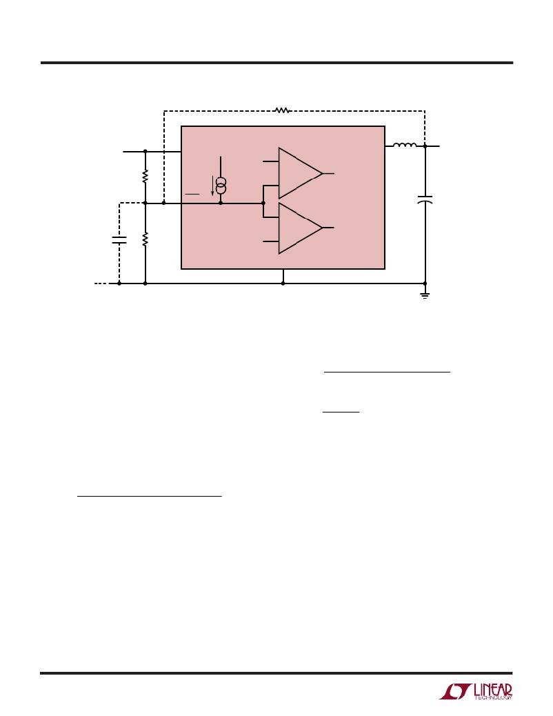
�Figure� 4.� Undervoltage� Lockout�
�1506� F04�
�[� (� )�
�(�
�)�
�(� )� =� 48� k�
�(�
�)�
�Keeptheconnectionsfromtheresistorstotheshutdown�
�pin� short� and� make� sure� that� interplane� or� surface� capaci-�
�tance� to� the� switching� nodes� are� minimized.� If� high�
�resistor� values� are� used,� the� shutdown� pin� should� be�
�bypassed� with� a� 1000pF� capacitor� to� prevent� coupling�
�problems� from� the� switch� node.� If� hysteresis� is� desired� in�
�the� undervoltage� lockout� point,� a� resistor� R� FB� can� be�
�added� to� the� output� node.� Resistor� values� can� be� calcu-�
�lated� from:�
�25� k� 6� ?� 2� .� 38� 1� .� 5� /� 5� +� 1� +� 1� .� 5�
�R� HI� =�
�2� .� 38� ?� 25� k� 3� .� 5� μ� A�
�25� k� 5� .� 2�
�=�
�2� .� 29�
�R� FB� =� 48� k� 5� /� 1� .� 5� =� 160� k�
�]�
�R� LO� [� IN� (� OUT� +� 1� )� +� ?� V�
�(�
�)�
�R� HI� =�
�V� ?� 2� .� 38� ?� V� /� V�
�2� .� 38� ?� R� 2� 3� .� 5� μ� A�
�R� FB� =� (� R� HI� )(� V� OUT� /� ?� V� )�
�]�
�SWITCH� NODE� CONSIDERATIONS�
�For� maximum� efficiency,� switch� rise� and� fall� times� are�
�made� as� short� as� possible.� To� prevent� radiation� and� high�
�frequency� resonance� problems,� proper� layout� of� the� com-�
�ponents� connected� to� the� switch� node� is� essential.� B� field�
�(magnetic)� radiation� is� minimized� by� keeping� catch� diode,�
�25k� suggested� for� R� LO�
�V� IN� =� Input� voltage� at� which� switching� stops� as� input�
�voltage� descends� to� trip� level�
�?� V� =� Hysteresis� in� input� voltage� level�
�Example:� output� voltage� is� 5V,� switching� is� to� stop� if� input�
�voltage� drops� below� 6V� and� should� not� restart� unless�
�input� rises� back� to� 7.5V.� ?� V� is� therefore� 1.5V� and� V� IN� =� 6V.�
�Let� R� LO� =� 25k.�
�14�
�switch� pin,� and� input� bypass� capacitor� leads� as� short� as�
�possible.� E� field� radiation� is� kept� low� by� minimizing� the�
�length� and� area� of� all� traces� connected� to� the� switch� pin�
�and� BOOST� pin.� A� ground� plane� should� always� be� used�
�under� the� switcher� circuitry� to� prevent� interplane� cou-�
�pling.� A� suggested� layout� for� the� critical� components� is�
�shown� in� Figure� 5.� Note� that� the� feedback� resistors� and�
�compensation� components� are� kept� as� far� as� possible�
�相关PDF资料 |
PDF描述 |
|---|---|
| UVR1H470MED1TD | CAP ALUM 47UF 50V 20% RADIAL |
| 50YXH56MEFCT16.3X11 | CAP ALUM 56UF 50V 20% RADIAL |
| HM53-40360HLF | HIGH POWER LOW COST INDUCTORS |
| LT1506CS8#TR | IC REG BUCK ADJ 4.5A 8SOIC |
| GBA30DRMT-S288 | CONN EDGECARD 60POS .125 EXTEND |
相关代理商/技术参数 |
参数描述 |
|---|---|
| LT1506G | 制造商:DIODES 制造商全称:Diodes Incorporated 功能描述:1.5A GLASS PASSIVATED RECTIFIER |
| LT1506I | 制造商:LINER 制造商全称:Linear Technology 功能描述:4.5A, 500kHz Step-Down Switching Regulator |
| LT1506IR | 功能描述:IC REG BUCK ADJ 4.5A D2PAK RoHS:否 类别:集成电路 (IC) >> PMIC - 稳压器 - DC DC 开关稳压器 系列:- 设计资源:Design Support Tool 标准包装:1 系列:- 类型:升压(升压) 输出类型:固定 输出数:1 输出电压:3V 输入电压:0.75 V ~ 2 V PWM 型:- 频率 - 开关:- 电流 - 输出:100mA 同步整流器:是 工作温度:-40°C ~ 85°C 安装类型:表面贴装 封装/外壳:SOT-23-5 细型,TSOT-23-5 包装:剪切带 (CT) 供应商设备封装:TSOT-23-5 其它名称:AS1323-BTTT-30CT |
| LT1506IR#PBF | 功能描述:IC REG BUCK ADJ 4.5A D2PAK RoHS:是 类别:集成电路 (IC) >> PMIC - 稳压器 - DC DC 开关稳压器 系列:- 标准包装:250 系列:- 类型:降压(降压) 输出类型:固定 输出数:1 输出电压:1.2V 输入电压:2.05 V ~ 6 V PWM 型:电压模式 频率 - 开关:2MHz 电流 - 输出:500mA 同步整流器:是 工作温度:-40°C ~ 85°C 安装类型:表面贴装 封装/外壳:6-UFDFN 包装:带卷 (TR) 供应商设备封装:6-SON(1.45x1) 产品目录页面:1032 (CN2011-ZH PDF) 其它名称:296-25628-2 |
| LT1506IR#TR | 功能描述:IC REG BUCK ADJ 4.5A D2PAK RoHS:否 类别:集成电路 (IC) >> PMIC - 稳压器 - DC DC 开关稳压器 系列:- 设计资源:Design Support Tool 标准包装:1 系列:- 类型:升压(升压) 输出类型:固定 输出数:1 输出电压:3V 输入电压:0.75 V ~ 2 V PWM 型:- 频率 - 开关:- 电流 - 输出:100mA 同步整流器:是 工作温度:-40°C ~ 85°C 安装类型:表面贴装 封装/外壳:SOT-23-5 细型,TSOT-23-5 包装:剪切带 (CT) 供应商设备封装:TSOT-23-5 其它名称:AS1323-BTTT-30CT |
发布紧急采购,3分钟左右您将得到回复。