- 您现在的位置:买卖IC网 > PDF目录15983 > LT1510-5IGN#PBF (Linear Technology)IC BATT CHARGER CONST V/I 16SSOP PDF资料下载
参数资料
| 型号: | LT1510-5IGN#PBF |
| 厂商: | Linear Technology |
| 文件页数: | 6/16页 |
| 文件大小: | 0K |
| 描述: | IC BATT CHARGER CONST V/I 16SSOP |
| 标准包装: | 100 |
| 功能: | 充电管理 |
| 电池化学: | 锂离子,镍镉,镍氢 |
| 电源电压: | 6.2 V ~ 28 V |
| 工作温度: | -40°C ~ 85°C |
| 安装类型: | 表面贴装 |
| 封装/外壳: | 16-SSOP(0.154",3.90mm 宽) |
| 供应商设备封装: | 16-SSOP |
| 包装: | 管件 |
�� �
�
�LT1510/LT1510-5�
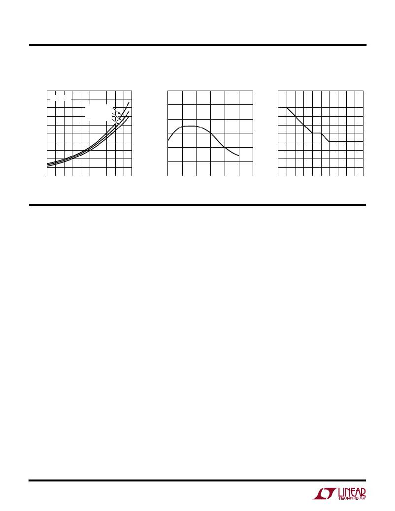
�TYPICAL� PERFOR� M� A� N� CE� CHARACTERISTICS�
�50�
�Switch� Current� vs� Boost� Current�
�vs� Boost� Voltage�
�2.470�
�Reference� Voltage� vs�
�Temperature�
�96�
�V� BOOST� vs�
�Maximum� Duty� Cycle�
�45�
�V� CC� = 16V�
�95�
�40�
�35�
�30�
�25�
�20�
�15�
�10�
�5�
�V� BOOST� =� 38V�
�28V�
�18V�
�2.468�
�2.466�
�2.464�
�2.462�
�2.460�
�94�
�93�
�92�
�91�
�90�
�89�
�88�
�87�
�0�
�0� 0.2� 0.4� 0.6� 0.8� 1.0� 1.2� 1.4� 1.6� 1.8� 2.0�
�2.458�
�0�
�25�
�50� 75� 100�
�125�
�150�
�86�
�2�
�4�
�6�
�8�
�10� 12� 14� 16� 18� 20� 22�
�SWITCH� CURRENT� (A)�
�PI� N� FU� N� CTIO� N� S�
�1510� G07�
�TEMPERATURE� (� °� C)�
�1510� G14�
�V� BOOST� (V)�
�LT1510� ?� TPC15�
�GND:� Ground� Pin.�
�SW:� Switch� Output.� The� Schottky� catch� diode� must� be�
�placed� with� very� short� lead� length� in� close� proximity� to� SW�
�pin� and� GND.�
�V� CC� :� Supply� for� the� Chip.� For� good� bypass,� a� low� ESR�
�capacitor� of� 10� μ� F� or� higher� is� required,� with� the� lead� length�
�kept� to� a� minimum.� V� CC� should� be� between� 8V� and� 28V�
�and� at� least� 2V� higher� than� V� BAT� for� V� BAT� less� than� 10V,� and�
�2.5V� higher� than� V� BAT� for� V� BAT� greater� than� 10V.� Under-�
�voltage� lockout� starts� and� switching� stops� when� V� CC� goes�
�below� 7V.� Note� that� there� is� a� parasitic� diode� inside� from�
�SW� pin� to� V� CC� pin.� Do� not� force� V� CC� below� SW� by� more�
�than� 0.7V� with� battery� present.� All� V� CC� pins� should� be�
�shorted� together� close� to� the� pins.�
�BOOST:� This� pin� is� used� to� bootstrap� and� drive� the� switch�
�power� NPN� transistor� to� a� low� on-voltage� for� low� power�
�dissipation.� In� normal� operation,� V� BOOST� =� V� CC� +� V� BAT�
�when� switch� is� on.� Maximum� allowable� V� BOOST� is� 55V.�
�SENSE:� Current� Amplifier� CA1� Input.� Sensing� can� be� at�
�either� terminal� of� the� battery.� Note� that� current� sense�
�resistor� R� S1� (0.08� ?� )� is� between� Sense� and� BAT� pins.�
�6�
�BAT:� Current� Amplifier� CA1� Input.�
�PROG:� This� pin� is� for� programming� the� charging� current�
�and� for� system� loop� compensation.� During� normal� opera-�
�tion,� V� PROG� stays� close� to� 2.465V.� If� it� is� shorted� to� GND�
�the� switching� will� stop.� When� a� microprocessor-controlled�
�DAC� is� used� to� program� charging� current,� it� must� be�
�capable� of� sinking� current� at� a� compliance� up� to� 2.465V.�
�V� C� :� This� is� the� control� signal� of� the� inner� loop� of� the� current�
�mode� PWM.� Switching� starts� at� 0.7V� and� higher� V� C�
�corresponds� to� higher� charging� current� in� normal� opera-�
�tion.� A� capacitor� of� at� least� 0.1� μ� F� to� GND� filters� out� noise�
�and� controls� the� rate� of� soft� start.� To� shut� down� switching,�
�pull� this� pin� low.� Typical� output� current� is� 30� μ� A.�
�OVP:� This� is� the� input� to� the� amplifier� VA� with� a� threshold�
�of� 2.465V.� Typical� input� current� is� about� 50nA� into� pin.� For�
�charging� lithium-ion� batteries,� VA� monitors� the� battery�
�voltage� and� reduces� charging� current� when� battery� volt-�
�age� reaches� the� preset� value.� If� it� is� not� used,� the� OVP� pin�
�should� be� grounded.�
�相关PDF资料 |
PDF描述 |
|---|---|
| ADM6710BARJZ-REEL7 | IC SUPERVISOR MPU SOT23-6 |
| RMC08DREI-S13 | CONN EDGECARD 16POS .100 EXTEND |
| A3RRB-4036M | IDC CABLE - APR40B/AE40M/APR40B |
| 100YXJ330MGC16X25 | CAP ALUM 330UF 100V 20% RADIAL |
| RP10-4805DE/M1-HC | CONV DC/DC 10W 36-75VIN +/-05V |
相关代理商/技术参数 |
参数描述 |
|---|---|
| LT-1510-610-006 | 制造商:Carling Technologies 功能描述:LT-SERIES TOGGLE SWITCH - Bulk |
| LT-1510-610-012 | 制造商:Carling Technologies 功能描述:LT-SERIES TOGGLE SWITCH - Bulk |
| LT-1510-610-125 | 制造商:Carling Technologies 功能描述:LT-SERIES TOGGLE SWITCH - Bulk |
| LT-1510-612-250 | 制造商:Carling Technologies 功能描述:LT-SERIES TOGGLE SWITCH - Bulk |
| LT1510614012 | 制造商:CARLING 功能描述:* |
发布紧急采购,3分钟左右您将得到回复。