参数资料
| 型号: | LT1528CQ#TR |
| 厂商: | Linear Technology |
| 文件页数: | 8/12页 |
| 文件大小: | 0K |
| 描述: | IC REG LDO 3.3V/ADJ 3A DDPAK5 |
| 标准包装: | 750 |
| 稳压器拓扑结构: | 正,固定式和可调式 |
| 输出电压: | 3.3V,3.3 V ~ 14.15 V |
| 输入电压: | 3.9 V ~ 15 V |
| 电压 - 压降(标准): | 0.57V @ 3A |
| 稳压器数量: | 1 |
| 电流 - 输出: | 3A |
| 电流 - 限制(最小): | 3.2A |
| 工作温度: | 0°C ~ 125°C |
| 安装类型: | 表面贴装 |
| 封装/外壳: | TO-263-6,D²Pak(5 引线+接片),TO-263BA |
| 供应商设备封装: | D2PAK-5 |
| 包装: | 带卷 (TR) |
�� �
�
�LT1528�
�APPLICATIONS� INFORMATION�
�The� LT1528� is� speci?ed� with� the� SENSE� pin� tied� to�
�the� OUTPUT� pin.� This� sets� the� output� voltage� to� 3.3V.�
�Speci?cations� for� output� voltage� greater� than� 3.3V� will�
�be� proportional� to� the� ratio� of� the� desired� output� voltage�
�to� 3.3V� (V� OUT� /3.3V).� For� example,� load� regulation� for� an�
�output� current� change� of� 1mA� to� 1.5A� is� –� 5mV� (typical)� at�
�V� OUT� =� 3.3V.� At� V� OUT� =� 12V,� load� regulation� would� be:�
�(12V/3.3V)� ?� (–5mV)� =� (–18mV)�
�Thermal� Considerations�
�The� power� handling� capability� of� the� device� will� be� limited�
�by� the� maximum� rated� junction� temperature� (125°C).� The�
�Table� 1a� lists� thermal� resistance� for� the� DD� package.�
�For� the� TO-220� package� (Table� 1b)� thermal� resistance� is�
�given� for� junction-to-case� only� since� this� package� is� usu-�
�ally� mounted� to� a� heat� sink.� Measured� values� of� thermal�
�resistance� for� several� different� copper� areas� are� listed� for�
�the� DD� package.� All� measurements� were� taken� in� still� air�
�on� 3/32"� FR-4� board� with� one� ounce� copper.� This� data�
�can� be� used� as� a� rough� guideline� in� estimating� thermal�
�resistance.� The� thermal� resistance� for� each� application� will�
�be� affected� by� thermal� interactions� with� other� components�
�as� well� as� board� size� and� shape.� Some� experimentation�
�will� be� necessary� to� determine� the� actual� value.�
�power� dissipated� by� the� device� will� be� made� up� of� two�
�components:�
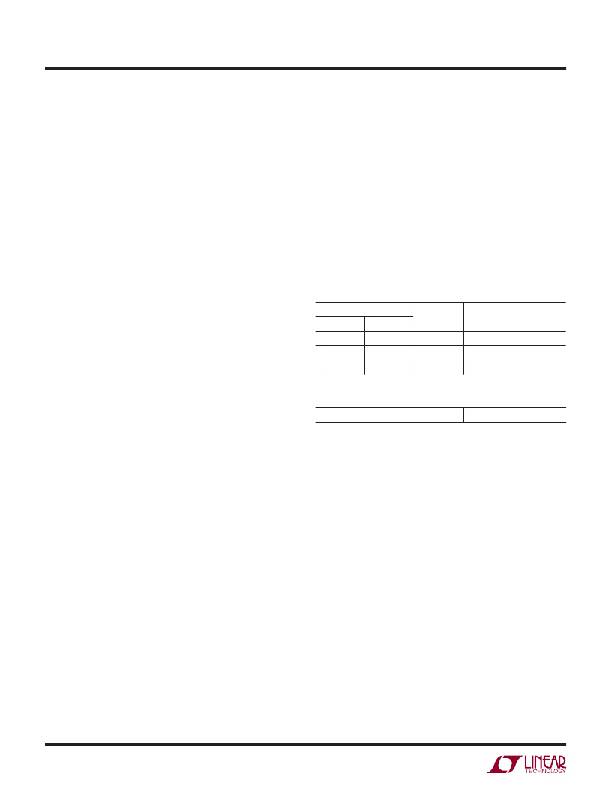
�Table� 1a.� Q-Package,� 5-Lead� DD�
�COPPER� AREA�
�THERMAL� RESISTANCE�
�1.� Output� current� multiplied� by� the� input/output� voltage�
�TOPSIDE*�
�BACKSIDE� BOARD AREA� (JUNCTION-TO-AMBIENT)�
�differential,� I� OUT� ?� (V� IN� –� V� OUT� ),� and�
�2.� GND� pin� current� multiplied� by� the� input� voltage,�
�I� GND� ?� V� IN.�
�The� GND� pin� current� can� be� found� by� examining� the� GND�
�Pin� Current� curves� in� the� Typical� Performance� Character-�
�istics.� Power� dissipation� will� be� equal� to� the� sum� of� the�
�2500� sq� mm� 2500� sq� mm� 2500� sq� mm�
�1000� sq� mm� 2500� sq� mm� 2500� sq� mm�
�125� sq� mm� 2500� sq� mm� 2500� sq� mm�
�*Device� is� mounted� on� topside.�
�Table� 1b.� T� Package,� 5-Lead� TO-220�
�Thermal� Resistance� (Junction-to-Case)�
�23°C/W�
�25°C/W�
�33°C/W�
�2.5°C/W�
�two� components� listed� above.�
�The� LT1528� has� internal� thermal� limiting� designed� to� pro-�
�tect� the� device� during� overload� conditions.� For� continuous�
�normal� load� conditions� the� maximum� junction� temperature�
�rating� of� 125°C� must� not� be� exceeded.� It� is� important� to�
�give� careful� consideration� to� all� sources� of� thermal� resis-�
�tance� from� junction-to-ambient.� Additional� heat� sources�
�mounted� nearby� must� also� be� considered.�
�For� surface� mount� devices� heat� sinking� is� accomplished�
�by� using� the� heat� spreading� capabilities� of� the� PC� board�
�and� its� copper� traces.� Experiments� have� shown� that� the�
�heat� spreading� copper� layer� does� not� have� to� be� electri-�
�cally� connected� to� the� tab� of� the� device.� The� PC� material�
�can� be� very� effective� at� transmitting� heat� between� the�
�pad� area,� attached� to� the� tab� of� the� device,� and� a� ground�
�or� power� plane� either� inside� or� on� the� opposite� side� of�
�the� board.� Although� the� actual� thermal� resistance� of� the�
�PC� material� is� high,� the� length/area� ratio� of� the� thermal�
�resistor� between� layers� is� small.� Copper� board� stiffeners�
�and� plated� through� holes� can� also� be� used� to� spread� the�
�Calculating� Junction� Temperature�
�Example:� Given� an� output� voltage� of� 3.3V,� an� input� voltage�
�range� of� 4.5V� to� 5.5V,� an� output� current� range� of� 0mA� to�
�500mA� and� a� maximum� ambient� temperature� of� 50°C,�
�what� will� the� maximum� junction� temperature� be?�
�The� power� dissipated� by� the� device� will� be� equal� to:�
�I� OUT(MAX)� ?� (V� IN(MAX)� –� V� OUT� )� +� [I� GND� ?� V� IN(MAX)� ]�
�where,�
�I� OUT(MAX)� =� 500mA�
�V� IN(MAX)� =� 5.5V�
�I� GND� at� (I� OUT� =� 500mA,� V� IN� =� 5.5V)� =� 4mA�
�so,�
�P� =� 500mA� ?� (5.5V� –� 3.3V)� +� (4mA� ?� 5.5V)� =� 1.12W�
�If� we� use� a� DD� package,� the� thermal� resistance� will� be� in�
�the� range� of� 23°C/W� to� 33°C/W� depending� on� the� copper�
�area.� So� the� junction� temperature� rise� above� ambient� will�
�be� approximately� equal� to:�
�1.12W� ?� 28°C/W� =� 31.4°C�
�heat� generated� by� power� devices.�
�1528fb�
�8�
�相关PDF资料 |
PDF描述 |
|---|---|
| ABB65DHRR | CONN CARD EXTEND 130POS .050" |
| AMM25DSUS | CONN EDGECARD 50POS .156 DIP SLD |
| AMM25DRUS | CONN EDGECARD 50POS .156 DIP SLD |
| ABM40DRMT-S288 | CONN EDGECARD EXTEND 80POS .156 |
| AMM25DSES-S243 | CONN EDGECARD 50POS .156 EYELET |
相关代理商/技术参数 |
参数描述 |
|---|---|
| LT1528CT | 功能描述:IC REG LDO 3.3V/ADJ 3A TO220-5 RoHS:否 类别:集成电路 (IC) >> PMIC - 稳压器 - 线性 系列:- 标准包装:1 系列:- 稳压器拓扑结构:正,固定式 输出电压:3V 输入电压:2.3 V ~ 5.5 V 电压 - 压降(标准):0.035V @ 150mA 稳压器数量:2 电流 - 输出:150mA 电流 - 限制(最小):300mA 工作温度:-40°C ~ 125°C 安装类型:表面贴装 封装/外壳:6-UFDFN 裸露焊盘,6-TMLF? 供应商设备封装:6-TMLF?(1.6x1.6) 包装:Digi-Reel® 产品目录页面:1104 (CN2011-ZH PDF) 其它名称:576-3018-6 |
| LT1528CT#PBF | 功能描述:IC REG LDO 3.3V/ADJ 3A TO220-5 RoHS:是 类别:集成电路 (IC) >> PMIC - 稳压器 - 线性 系列:- 标准包装:1 系列:- 稳压器拓扑结构:正,固定式 输出电压:8V 输入电压:10.5 V ~ 23 V 电压 - 压降(标准):1.7V @ 40mA 稳压器数量:1 电流 - 输出:100mA(最小值) 电流 - 限制(最小):- 工作温度:0°C ~ 125°C 安装类型:表面贴装 封装/外壳:8-SOIC(0.154",3.90mm 宽) 供应商设备封装:8-SOIC 包装:剪切带 (CT) 产品目录页面:1075 (CN2011-ZH PDF) 其它名称:296-24390-1 |
| LT1528CTPBF | 制造商:Linear Technology 功能描述:LDO Regulator 3.3V 3A Fast TO220-5 |
| LT1529 | 制造商:Linear Technology 功能描述: |
| LT1529-3.3 | 制造商:LINER 制造商全称:Linear Technology 功能描述:3A Low Dropout Regulators with Micropower Quiescent Current and Shutdown |
发布紧急采购,3分钟左右您将得到回复。