- 您现在的位置:买卖IC网 > PDF目录377707 > LT1529IT-3.3 (LINEAR TECHNOLOGY CORP) Cap-Free, NMOS, 150mA Low Dropout Regulator with Reverse Current Protection PDF资料下载
参数资料
| 型号: | LT1529IT-3.3 |
| 厂商: | LINEAR TECHNOLOGY CORP |
| 元件分类: | 基准电压源/电流源 |
| 英文描述: | Cap-Free, NMOS, 150mA Low Dropout Regulator with Reverse Current Protection |
| 中文描述: | 3.3 V FIXED POSITIVE LDO REGULATOR, 0.5 V DROPOUT, PSFM5 |
| 封装: | PLASTIC, TO-220, 5 PIN |
| 文件页数: | 3/12页 |
| 文件大小: | 139K |
| 代理商: | LT1529IT-3.3 |
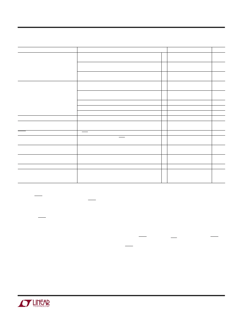
3
LT1529
LT1529-3.3/LT1529-5
ELECTRICAL C
The
G
denotes specifications which apply over the operating temperature range, otherwise specificatons are at T
A
= 25
°
C. (Note 3)
HARA TERISTICS
PARAMETER
Dropout Voltage
(Note 6)
CONDITIONS
I
LOAD
= 700mA, T
J
= 25
°
C
I
LOAD
= 700mA
I
LOAD
= 1.5A, T
J
= 25
°
C
I
LOAD
= 1.5A
I
LOAD
= 3A, T
J
= 25
°
C
I
LOAD
= 3A
I
LOAD
= 0mA, T
J
= 25
°
C
I
LOAD
= 0mA, T
J
= 125
°
C (Note 8)
I
LOAD
= 100mA, T
J
= 25
°
C
I
LOAD
= 100mA, T
J
= 125
°
C (Note 8)
I
LOAD
= 700mA
I
LOAD
= 1.5A
I
LOAD
= 3A
T
J
= 25
°
C
V
OUT
= Off to On
V
OUT
= On to Off
V
SHDN
= 0V
V
IN
= V
OUT
(Nominal) + 1V, V
SHDN
= 0V
MIN
TYP
320
MAX
430
550
550
700
750
950
100
UNITS
mV
mV
mV
mV
mV
mV
G
430
G
600
G
GND Pin Current
(Note 7)
50
400
0.6
1.0
5.5
20
80
150
1.20
0.75
4.5
15
μ
A
μ
A
mA
mA
mA
mA
mA
nA
1.0
G
12
40
160
300
2.8
G
G
ADJ Pin Bias Current (Notes 5, 9)
Shutdown Threshold
G
G
V
V
0.25
SHDN Pin Current (Note 10)
Quiescent Current in Shutdown
(Note 11)
Ripple Rejection
G
10
30
μ
A
μ
A
G
V
IN
– V
OUT
= 1V (Avg), V
RIPPLE
= 0.5V
P-P
,
f
RIPPLE
= 120Hz, I
LOAD
= 1.5A
V
IN
– V
OUT
= 7V, T
J
= 25
°
C
V
IN
= V
OUT
(Nominal) + 1.5V,
V
OUT
= –0.1V
V
IN
= –15V, V
OUT
= 0V
LT1529-3.3
LT1529-5
LT1529 (Note 6)
50
62
dB
Current Limit
5
A
A
G
3.2
4.7
Input Reverse Leakage Current
Reverse Output Current (Note 12)
G
1.0
mA
μ
A
μ
A
μ
A
V
OUT
= 3.3V, V
IN
= 0V
V
OUT
= 5V, V
IN
= 0V
V
OUT
= 3.8V, V
IN
= 0V
16
16
16
Note 1:
Absolute Maximum Ratings are those values beyond which the life
of a device may be impaired.
Note 2:
The SHDN pin input voltage rating is required for a low impedance
source. Internal protection devices connected to the SHDN pin will turn on
and clamp the pin to approximately 7V or –0.6V. This range allows the use
of 5V logic devices to drive the pin directly. For high impedance sources or
logic running on supply voltages greater than 5.5V, the maximum current
driven into the SHDN pin must be limited to less than 5mA.
Note 3:
The device is tested under pulse load conditions such that T
J
= T
A
.
Note 4:
Operating conditions are limited by maximum junction
temperature. The regulated output voltage specification will not apply for
all possible combinations of input voltage and output current. When
operating at maximum input voltage, the output current range must be
limited. When operating at maximum output current the input voltage
range must be limited.
Note 5:
The LT1529 is tested and specified with the ADJ pin connected to
the OUTPUT pin.
Note 6:
Dropout voltage is the minimum input/output voltage required to
maintain regulation at the specified output current. In dropout the output
voltage will be equal to (V
IN
– V
DROPOUT
).
Note 7:
GND pin current is tested with V
IN
= V
OUT
(nominal) and a current
source load. This means that the device is tested while operating in its
dropout region. This is the worst-case GND pin current. The GND pin
current will decrease slightly at higher input voltages.
Note 8:
GND pin current will rise at T
J
> 75
°
C. This is due to internal
circuitry designed to compensate for leakage currents in the output
transistor at high temperatures. This allows quiescent current to be
minimized at lower temperatures, yet maintain output regulation at high
temperatures with light loads. See quiescent current curve in typical
performance characteristics.
Note 9:
ADJ pin bias current flows into the ADJ pin.
Note 10:
SHDN pin current at V
SHDN
= 0V flows out of the SHDN pin.
Note 11:
Quiescent current in shutdown is equal to the sum total of the
SHDN pin current (5
μ
A) and the GND pin current (10
μ
A).
Note 12:
Reverse output current is tested with the V
IN
pin grounded and
the OUTPUT pin forced to the rated output voltage. This current flows into
the OUTPUT pin and out of the GND pin.
相关PDF资料 |
PDF描述 |
|---|---|
| LT1529IT-5 | Cap-Free, NMOS, 150mA Low Dropout Regulator with Reverse Current Protection |
| LT1534IS-1 | RADIATION HARDENED HIGH EFFICIENCY, 5 AMP SWITCHING REGULATORS |
| LT1534-1 | RADIATION HARDENED HIGH EFFICIENCY, 5 AMP SWITCHING REGULATORS |
| LT1534CS-1 | RADIATION HARDENED HIGH EFFICIENCY, 5 AMP SWITCHING REGULATORS |
| LT1534 | Octal Bus Transceivers 20-PDIP 0 to 70 |
相关代理商/技术参数 |
参数描述 |
|---|---|
| LT1529IT-5 | 功能描述:IC REG LDO 5V 3A TO220-5 RoHS:否 类别:集成电路 (IC) >> PMIC - 稳压器 - 线性 系列:- 标准包装:1 系列:- 稳压器拓扑结构:正,固定式 输出电压:3V 输入电压:2.3 V ~ 5.5 V 电压 - 压降(标准):0.035V @ 150mA 稳压器数量:2 电流 - 输出:150mA 电流 - 限制(最小):300mA 工作温度:-40°C ~ 125°C 安装类型:表面贴装 封装/外壳:6-UFDFN 裸露焊盘,6-TMLF? 供应商设备封装:6-TMLF?(1.6x1.6) 包装:Digi-Reel® 产品目录页面:1104 (CN2011-ZH PDF) 其它名称:576-3018-6 |
| LT1529IT-5#PBF | 功能描述:IC REG LDO 5V 3A TO220-5 RoHS:是 类别:集成电路 (IC) >> PMIC - 稳压器 - 线性 系列:- 标准包装:1 系列:- 稳压器拓扑结构:正,固定式 输出电压:3V 输入电压:2.3 V ~ 5.5 V 电压 - 压降(标准):0.035V @ 150mA 稳压器数量:2 电流 - 输出:150mA 电流 - 限制(最小):300mA 工作温度:-40°C ~ 125°C 安装类型:表面贴装 封装/外壳:6-UFDFN 裸露焊盘,6-TMLF? 供应商设备封装:6-TMLF?(1.6x1.6) 包装:Digi-Reel® 产品目录页面:1104 (CN2011-ZH PDF) 其它名称:576-3018-6 |
| LT-1530-110-012 | 制造商:Carling Technologies 功能描述:SINGLE-POLE, LIGHTED TOGGLE, RED LENS - Bulk |
| LT-1530-110-018 | 制造商:Carling Technologies 功能描述:LT-SERIES TOGGLE SWITCH - Bulk |
发布紧急采购,3分钟左右您将得到回复。