- 您现在的位置:买卖IC网 > PDF目录377707 > LT1534 (Linear Technology Corporation) Octal Bus Transceivers 20-PDIP 0 to 70 PDF资料下载
参数资料
| 型号: | LT1534 |
| 厂商: | Linear Technology Corporation |
| 英文描述: | Octal Bus Transceivers 20-PDIP 0 to 70 |
| 中文描述: | 超低噪声甲开关稳压器 |
| 文件页数: | 10/16页 |
| 文件大小: | 222K |
| 代理商: | LT1534 |
10
LT1534/LT1534-1
APPLICATIO
S I
N
FOR
ATIO
U
One word of caution. Sometimes a feedback zero is added
to the control loop by placing a capacitor across R1 above.
If the feedback zero capacitively pulls the FB pin above the
internal regulator voltage (2.4V typ), output regulation
may be disrupted. A series resistance with the feedback
pin can eliminate this potential problem.
W
U
Thermal Considerations
Computing power dissipation for this IC requires careful
attention to detail. Reduced output slewing causes the part
to dissipate more power than would occur with fast edges.
However, much improvement in noise can be produced
with modest decrease in supply efficiency.
Power dissipation is a function of topology, input voltage,
switch current and slew rates. It is impractical to come up
with an all-encompassing formula. It is therefore recom-
mended that package temperature be measured in each
application. The part has an internal thermal shutdown to
prevent device destruction, but this should not replace
careful thermal design.
1. Dissipation due to input current:
P
V
mA
I
VIN
IN
=
+
11
60
where I is the average switch current.
2. Dissipation due to the driver saturation:
P
VSAT
= (V
SAT
)(I)(DC
MAX
)
where V
SAT
is the output saturation voltage which is
approximately 0.1 + (0.2)(I), DC
MAX
is the maximum
duty cycle.
3. Dissipation due to output slew using approximations
for slew rates:
P
V
I
I
R
I V
()
V
R
f
SLEW
IN
CSL
IN
SAT
4
VSL
OSC
=
( )
( )
+
(
)
+
(
(
)
(
)
2
2
9
2
2
9
4
220 10
Note if V
SAT
and
I are small with respect to V
IN
and I,
then:
P
()(
( )
V
R
f
V
I
SLEW
CSL
VSL
OSC
IN
=
)
+
( )(
(
)
(
)( )()
220 10
9
9
Negative Output Voltage Setting
Negative output voltage can be sensed using the NFB pin.
In this case regulation will occur when the NFB pin is at
–2.5V. The input bias current for the NFB pin is –25
μ
A
(I
NFB
) and must be accounted for when selecting divider
resistor values.
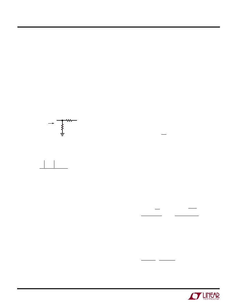
Figure 3
NFB PIN
I
NFB
1534 F02
–V
OUT
R2
R1
Referring to Figure 3, R1 is chosen such that:
R
R
V
R
A
OUT
+
1
2
2 5
.
2 5
.
2 25
=
μ
A suggested value for R2 is 2.5k. The NFB pin is normally
left open if the FB pin is being used.
Dual Polarity Output Voltage Sensing
Certain applications may benefit from sensing both posi-
tive and negative output voltages. When doing this each
output voltage resistor divider is individually set as previ-
ously described. When both FB and NFB pins are used, the
LT1534 will act to prevent either output from going
beyond its set output voltage. The highest output (lightest
load) will dominate control of the regulator. This technique
would prevent either output from going unregulated high
at no load. However, this technique will also compromise
output load regulation.
Shutdown
If the shutdown pin is pulled low, the regulator will turn off.
The supply current will be reduced to less than 20
μ
A.
相关PDF资料 |
PDF描述 |
|---|---|
| LT1534C | RADIATION HARDENED HIGH EFFICIENCY, 5 AMP SWITCHING REGULATORS |
| LT1534CS | RADIATION HARDENED HIGH EFFICIENCY, 5 AMP SWITCHING REGULATORS |
| LT1534I | RADIATION HARDENED HIGH EFFICIENCY, 5 AMP SWITCHING REGULATORS |
| LT1534IS | RADIATION HARDENED HIGH EFFICIENCY, 5 AMP SWITCHING REGULATORS |
| LT1537C | Advanced Low Power 5V RS232 Transceiver with Small Capacitors |
相关代理商/技术参数 |
参数描述 |
|---|---|
| LT1534-1 | 制造商:LINER 制造商全称:Linear Technology 功能描述:Ultralow Noise 2A Switching Regulators |
| LT-1534-501-024 | 制造商:Carling Technologies 功能描述:LT-SERIES TOGGLE SWITCH - Bulk |
| LT-1534-510-012 | 制造商:Carling Technologies 功能描述:LT-SERIES TOGGLE SWITCH - Bulk |
| LT-1534-510-024 | 制造商:Carling Technologies 功能描述:LT-SERIES TOGGLE SWITCH - Bulk |
| LT-1534-510-125 | 制造商:Carling Technologies 功能描述:LT-SERIES TOGGLE SWITCH - Bulk |
发布紧急采购,3分钟左右您将得到回复。