- 您现在的位置:买卖IC网 > PDF目录13125 > LT1580CR-2.5#PBF (Linear Technology)IC LDO REGULATOR 7A 2.5V DDPAK-7 PDF资料下载
参数资料
| 型号: | LT1580CR-2.5#PBF |
| 厂商: | Linear Technology |
| 文件页数: | 10/16页 |
| 文件大小: | 0K |
| 描述: | IC LDO REGULATOR 7A 2.5V DDPAK-7 |
| 产品培训模块: | More Information on LDOs |
| 标准包装: | 50 |
| 应用: | 转换器,Intel Pentium? |
| 输入电压: | 1.79 V ~ 6 V |
| 输出数: | 1 |
| 输出电压: | 2.5V |
| 工作温度: | 0°C ~ 125°C |
| 安装类型: | 表面贴装 |
| 封装/外壳: | TO-263-8,D²Pak(7 引线+接片),TO-263CA |
| 供应商设备封装: | D2PAK-7 |
| 包装: | 管件 |
| 产品目录页面: | 1328 (CN2011-ZH PDF) |
�� �
�
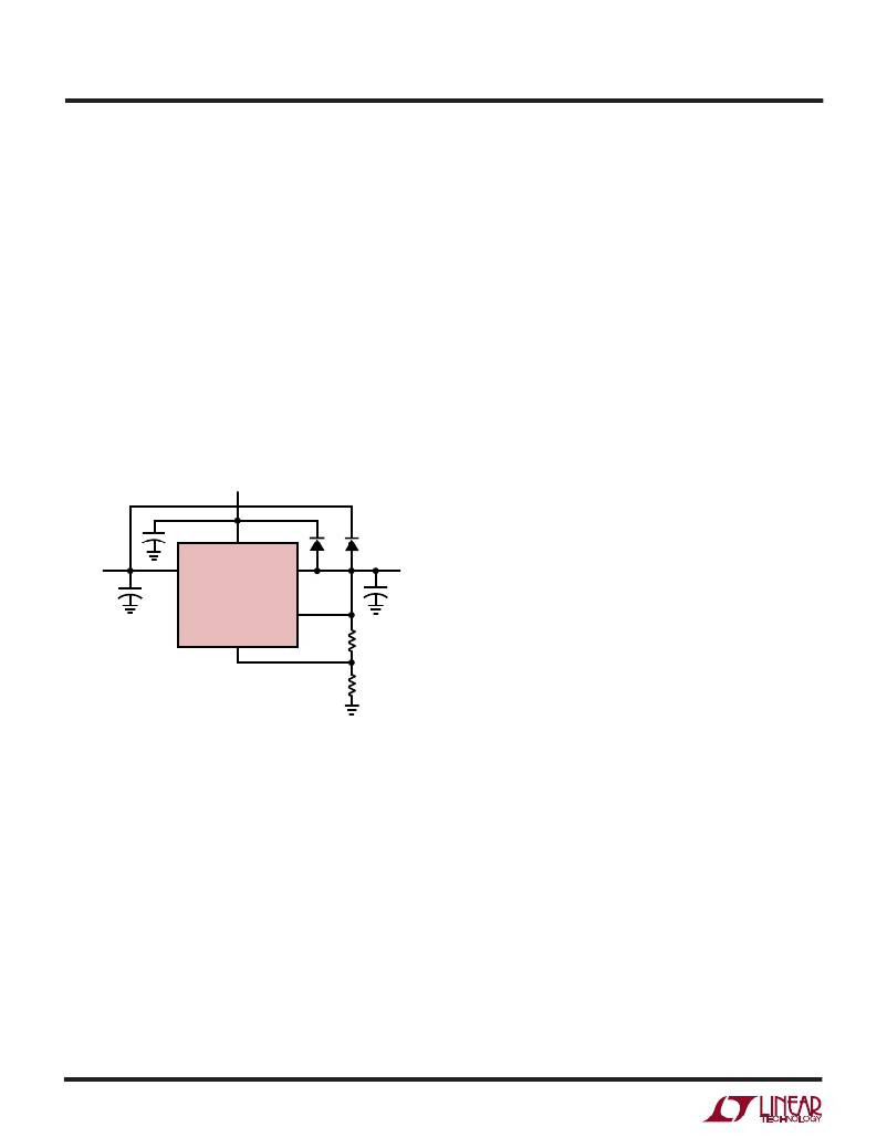
�LT1580/LT1580-2.5�
�APPLICATIO� N� S� I� N� FOR� M� ATIO� N�
�A� protection� diode� between� the� V� OUT� pin� and� the� V� POWER�
�pin� is� usually� not� needed.� An� internal� diode� between� the�
�V� OUT� pin� and� the� V� POWER� pin� on� the� LT1580� can� handle�
�microsecond� surge� currents� of� 50A� to� 100A.� Even� with�
�large� value� output� capacitors� it� is� difficult� to� obtain� those�
�values� of� surge� currents� in� normal� operation.� Only� with�
�large� values� of� output� capacitance,� such� as� 1000� μ� F� to�
�5000� μ� F,� and� with� the� V� POWER� pin� instantaneously� shorted�
�to� ground� can� damage� occur.� A� crowbar� circuit� at� the�
�power� input� can� generate� those� levels� of� current,� and� a�
�diode� from� output� to� power� input� is� then� recommended.�
�This� is� shown� in� Figure� 6.� Normal� power� supply� cycling� or�
�system� “hot� plugging� and� unplugging”� will� not� do� any�
�damage.�
�V� CONTROL�
�+�
�If� the� LT1580� is� connected� as� a� single� supply� device� with�
�the� V� CONTROL� and� V� POWER� input� pins� shorted� together� the�
�internal� diode� between� the� V� OUT� and� the� V� POWER� input� pin�
�will� protect� the� V� CONTROL� input� pin.�
�Like� any� other� regulator� exceeding� the� maximum� input� to�
�output� differential� can� cause� the� internal� transistors� to�
�break� down� and� none� of� the� internal� protection� circuitry� is�
�then� functional.�
�Thermal� Considerations�
�The� LT1580� has� internal� current� and� thermal� limiting�
�designed� to� protect� the� device� under� overload� conditions.�
�For� continuous� normal� load� conditions� maximum� junction�
�temperature� ratings� must� not� be� exceeded.� It� is� important�
�to� give� careful� consideration� to� all� sources� of� thermal�
�resistance� from� junction� to� ambient.� This� includes� junc-�
�tion-to-case,� case-to-heat� sink� interface� and� heat� sink�
�resistance� itself.� Thermal� resistance� specifications� are�
�+�
�V� CONTROL�
�V� POWER� V� POWER�
�LT1580�
�ADJ�
�*OPTIONAL� DIODES:� 1N4002�
�V� OUT�
�SENSE�
�D1*�
�D2*�
�+�
�R1�
�R2�
�V� OUT�
�given� in� the� electrical� characteristics� for� both� the� Control�
�section� and� the� Power� section� of� the� device.� The� thermal�
�resistance� of� the� Control� section� is� given� as� 0.65� °� C/W� and�
�junction� temperature� of� the� Control� section� is� allowed� to�
�run� at� up� to� 125� °� C.� The� thermal� resistance� of� the� Power�
�section� is� given� as� 2.7� °� C/W� and� the� junction� temperature�
�of� the� Power� section� is� allowed� to� run� at� up� to� 150� °� C.� The�
�difference� in� thermal� resistances� between� Control� and�
�1580� F06�
�Figure� 6.� Optional� Clamp� Diodes� Protect� Against�
�Input� Crowbar� Circuits�
�A� protection� diode� between� the� V� OUT� pin� and� the� V� CONTROL�
�pin� is� usually� not� needed.� An� internal� diode� between� the�
�V� OUT� pin� and� the� V� CONTROL� pin� on� the� LT1580� can� handle�
�microsecond� surge� currents� of� 1A� to� 10A.� This� can� only�
�occur� if� the� V� CONTROL� pin� is� instantaneously� shorted� to�
�ground� with� a� crowbar� circuit� with� large� value� output�
�capacitors.� Since� the� V� CONTROL� pin� is� usually� a� low� current�
�supply,� this� condition� is� unlikely.� A� protection� diode� from�
�the� V� OUT� pin� to� the� V� CONTROL� pin� is� recommended� if� the�
�V� CONTROL� pin� can� be� instantaneously� shorted� to� ground.�
�This� is� shown� in� Figure� 6.� Normal� power� supply� cycling� or�
�system� “hot� plugging� and� unplugging”� will� not� do� any�
�damage.�
�10�
�Power� sections� is� due� to� thermal� gradients� between� the�
�power� transistor� and� the� control� circuitry.�
�Virtually� all� of� the� power� dissipated� by� the� device� is�
�dissipated� in� the� power� transistor.� The� temperature� rise� in�
�the� power� transistor� will� be� greater� than� the� temperature�
�rise� in� the� Control� section� so� the� effective� thermal� resis-�
�tance,� temperature� rise� per� watt� dissipated,� will� be� lower�
�in� the� Control� section.� At� power� levels� below� 12W� the�
�temperature� gradient� will� be� less� than� 25� °� C� and� the�
�maximum� ambient� temperature� will� be� determined� by� the�
�junction� temperature� of� the� Control� section.� This� is� due� to�
�the� lower� maximum� junction� temperature� in� the� Control�
�section.� At� power� levels� greater� than� 12W� the� temperature�
�gradient� will� be� greater� than� 25� °� C� and� the� maximum�
�ambient� temperature� will� be� determined� by� the� Power�
�section.� For� both� cases� the� junction� temperature� is� deter-�
�mined� by� the� total� power� dissipated� in� the� device.� For� most�
�相关PDF资料 |
PDF描述 |
|---|---|
| ABC08DRAI-S734 | CONN EDGECARD 16POS .100 R/A PCB |
| ISL9012IRMNZ | IC REG LDO 3V/3.3V 10-DFN |
| RPR20-2405S-1 | CONV DC/DC 20W 12-36VIN 05VOUT |
| RMM15DRSD-S273 | CONN EDGECARD 30POS DIP .156 SLD |
| VI-B1H-EU-F1 | CONVERTER MOD DC/DC 52V 200W |
相关代理商/技术参数 |
参数描述 |
|---|---|
| LT1580CT | 功能描述:IC LDO REGULATOR 7A ADJ TO220-5 RoHS:否 类别:集成电路 (IC) >> PMIC - 稳压器 - 专用型 系列:- 标准包装:43 系列:- 应用:控制器,Intel VR11 输入电压:5 V ~ 12 V 输出数:1 输出电压:0.5 V ~ 1.6 V 工作温度:-40°C ~ 85°C 安装类型:表面贴装 封装/外壳:48-VFQFN 裸露焊盘 供应商设备封装:48-QFN(7x7) 包装:管件 |
| LT1580CT#06 | 制造商:Linear Technology 功能描述:7A Low Dropout HS Volt Reg |
| LT1580CT#06PBF | 功能描述:IC CONV PENTIUM PROCESSR TO220-5 RoHS:是 类别:集成电路 (IC) >> PMIC - 稳压器 - 专用型 系列:- 标准包装:43 系列:- 应用:控制器,Intel VR11 输入电压:5 V ~ 12 V 输出数:1 输出电压:0.5 V ~ 1.6 V 工作温度:-40°C ~ 85°C 安装类型:表面贴装 封装/外壳:48-VFQFN 裸露焊盘 供应商设备封装:48-QFN(7x7) 包装:管件 |
| LT1580CT#PBF | 功能描述:IC LDO REGULATOR 7A ADJ TO220-5 RoHS:是 类别:集成电路 (IC) >> PMIC - 稳压器 - 专用型 系列:- 标准包装:2,000 系列:- 应用:控制器,DSP 输入电压:4.5 V ~ 25 V 输出数:2 输出电压:最低可调至 1.2V 工作温度:-40°C ~ 85°C 安装类型:表面贴装 封装/外壳:30-TFSOP(0.173",4.40mm 宽) 供应商设备封装:30-TSSOP 包装:带卷 (TR) |
| LT1580CT33 | 制造商:LT 功能描述:* |
发布紧急采购,3分钟左右您将得到回复。