参数资料
| 型号: | LT1635IN8#PBF |
| 厂商: | Linear Technology |
| 文件页数: | 12/12页 |
| 文件大小: | 0K |
| 描述: | IC OPAMP/REF BUILD BLK R-R 8DIP |
| 标准包装: | 50 |
| 放大器类型: | 通用 |
| 电路数: | 2 |
| 输出类型: | 满摆幅 |
| 转换速率: | 0.05 V/µs |
| 增益带宽积: | 175kHz |
| 电流 - 输入偏压: | 2nA |
| 电压 - 输入偏移: | 300µV |
| 电流 - 电源: | 135µA |
| 电流 - 输出 / 通道: | 40mA |
| 电压 - 电源,单路/双路(±): | 1.2 V ~ 10 V,±0.6 V ~ 5 V |
| 工作温度: | -40°C ~ 85°C |
| 安装类型: | 通孔 |
| 封装/外壳: | 8-DIP(0.300",7.62mm) |
| 供应商设备封装: | 8-PDIP |
| 包装: | 管件 |
9
LT1635
The LT1635 is fully specified with V + = 5V, V – = 0V and
VCM = 2.5V. The op amp offset voltage is internally
trimmed to a minimum value at these supply voltages. A
unique feature of this device is that it operates from a
single 1.2V supply up to
±5V. A full set of specifications is
provided at
±5V supply voltages. The positive supply pin
of the LT1635 should be bypassed with a small capacitor
(about 0.1
F), as well as the negative supply pin when
using split supplies.
Op Amp
The LT1635 is fully specified for single supply operation,
i.e., when the negative supply is 0V. Input common mode
range of the op amp includes ground and the output
swings within a few millivolts of ground while sinking
current. The input stage of the op amp incorporates phase
reversal protection to prevent false outputs from occur-
ring when the input is below the negative supply. Protec-
tive resistors have been included in the input leads so that
current does not become excessive when the inputs are
forced below the negative supply.
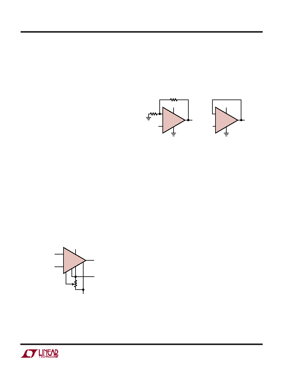
The op amp also includes an offset nulling feature, this is
accomplished by connecting the BALANCE pin (Pin 5) to
a variable voltage derived from the reference output. The
offset adjust range is asymmetrical, typically – 2mV to
8mV. At room temperature the input offset voltage of the
LT1635 is within the null range, thus the offset voltage can
be adjusted to zero. Figure 1 shows the standard offset
adjustment.
should be taken to keep the output from saturating. For
example, a 1mV input signal will cause the amplifier to set
up in its linear region in the gain 100 configuration as
shown in Figure 2a. However, 1mV is not enough to make
the amplifier function properly in the voltage follower mode
(Figure 2b).
Output
The output voltage swing of the LT1635 is a function of
input overdrive as shown in the typical performance curves.
When monitoring voltages within 15mV of either rail, gain
Distortion
There are two main contributors of distortion in op amps:
distortion caused by nonlinear common mode rejection
and output crossover distortion as the output transitions
from sourcing to sinking current. The common mode
rejection ratio of the LT1635 is very good, typically 110dB.
Therefore, as long as the input operates in normal com-
mon mode range, there will be very little common mode
induced distortion. Crossover distortion will increase as
the output load resistance decreases. For the lowest dis-
tortion, the LT1635 should be operated with the output
always sourcing current.
Reference
The reference of the LT1635 consists of a 200mV precision
bandgap and a reference amplifier. As shown in the block
diagram, the 0.2V precision bandgap is referred to V – and
is internally connected to the noninverting input of the ref-
erence amplifier. This configuration offers great flexibility
in that the reference voltage can be amplified or the reference
amplifier can be used as a comparator. Unlike the op amp,
the output of the reference amplifier can only swing within
0.8V (typ) of the positive rail. To guarantee that the reference
amplifier does not saturate over the industrial temperature
range, the minimum operating supply should be 1.3V. The
reference amplifier can source 2mA of load current and can
sink 10
A over the industrial temperature range.
Figure 2. Gain 100 Amplifier and Voltage Follower
–
+
LT1635
OP AMP
5V
99R
(a)
(b)
1mV
100mV
R
–
+
5V
1mV
1635 F02
OUTPUT
SATURATED
≈2mV
LT1635
OP AMP
–
+
LT1635
R1
10k
5
V –
V +
1
8
VREF
6
4
2
3
1635 F01
Figure 1. Standard Offset Adjustment
APPLICATIO S I FOR ATIO
WU
UU
相关PDF资料 |
PDF描述 |
|---|---|
| LT1636IDD#TRPBF | IC OP AMP SGL R-R IN/OUT 8-DFN |
| LT1638CDD | IC OPAMP R-R IN/OUT DUAL 8DFN |
| LT1677IS8#PBF | IC OPAMP R-R I/O SGL LN 8SOIC |
| LT1678IS8 | IC OPAMP R-R I/O DUAL LN 8SOIC |
| LT1724CS#TRPBF | IC PREC OPAMP 200MHZ QUAD 14SOIC |
相关代理商/技术参数 |
参数描述 |
|---|---|
| LT1635IS8 | 功能描述:IC OPAMP/REF BUILD BLK R-R 8SOIC RoHS:否 类别:集成电路 (IC) >> Linear - Amplifiers - Instrumentation 系列:- 标准包装:50 系列:LinCMOS™ 放大器类型:通用 电路数:4 输出类型:- 转换速率:0.05 V/µs 增益带宽积:110kHz -3db带宽:- 电流 - 输入偏压:0.7pA 电压 - 输入偏移:210µV 电流 - 电源:57µA 电流 - 输出 / 通道:30mA 电压 - 电源,单路/双路(±):3 V ~ 16 V,±1.5 V ~ 8 V 工作温度:-40°C ~ 85°C 安装类型:表面贴装 封装/外壳:14-SOIC(0.154",3.90mm 宽) 供应商设备封装:14-SOIC 包装:管件 产品目录页面:865 (CN2011-ZH PDF) 其它名称:296-1834296-1834-5 |
| LT1635IS8#PBF | 功能描述:IC OPAMP/REF BUILD BLK R-R 8SOIC RoHS:是 类别:集成电路 (IC) >> Linear - Amplifiers - Instrumentation 系列:- 标准包装:50 系列:LinCMOS™ 放大器类型:通用 电路数:4 输出类型:- 转换速率:0.05 V/µs 增益带宽积:110kHz -3db带宽:- 电流 - 输入偏压:0.7pA 电压 - 输入偏移:210µV 电流 - 电源:57µA 电流 - 输出 / 通道:30mA 电压 - 电源,单路/双路(±):3 V ~ 16 V,±1.5 V ~ 8 V 工作温度:-40°C ~ 85°C 安装类型:表面贴装 封装/外壳:14-SOIC(0.154",3.90mm 宽) 供应商设备封装:14-SOIC 包装:管件 产品目录页面:865 (CN2011-ZH PDF) 其它名称:296-1834296-1834-5 |
| LT1635IS8#TR | 功能描述:IC OPAMP/REF R-R MICROPWR 8SOIC RoHS:否 类别:集成电路 (IC) >> Linear - Amplifiers - Instrumentation 系列:- 标准包装:50 系列:LinCMOS™ 放大器类型:通用 电路数:4 输出类型:- 转换速率:0.05 V/µs 增益带宽积:110kHz -3db带宽:- 电流 - 输入偏压:0.7pA 电压 - 输入偏移:210µV 电流 - 电源:57µA 电流 - 输出 / 通道:30mA 电压 - 电源,单路/双路(±):3 V ~ 16 V,±1.5 V ~ 8 V 工作温度:-40°C ~ 85°C 安装类型:表面贴装 封装/外壳:14-SOIC(0.154",3.90mm 宽) 供应商设备封装:14-SOIC 包装:管件 产品目录页面:865 (CN2011-ZH PDF) 其它名称:296-1834296-1834-5 |
| LT1635IS8#TRPBF | 功能描述:IC OPAMP/REF BUILD BLK R-R 8SOIC RoHS:是 类别:集成电路 (IC) >> Linear - Amplifiers - Instrumentation 系列:- 标准包装:50 系列:LinCMOS™ 放大器类型:通用 电路数:4 输出类型:- 转换速率:0.05 V/µs 增益带宽积:110kHz -3db带宽:- 电流 - 输入偏压:0.7pA 电压 - 输入偏移:210µV 电流 - 电源:57µA 电流 - 输出 / 通道:30mA 电压 - 电源,单路/双路(±):3 V ~ 16 V,±1.5 V ~ 8 V 工作温度:-40°C ~ 85°C 安装类型:表面贴装 封装/外壳:14-SOIC(0.154",3.90mm 宽) 供应商设备封装:14-SOIC 包装:管件 产品目录页面:865 (CN2011-ZH PDF) 其它名称:296-1834296-1834-5 |
| LT1636 | 制造商:LINER 制造商全称:Linear Technology 功能描述:Over-The-Top Micropower Rail-to-Rail Input and Output Op Amp |
发布紧急采购,3分钟左右您将得到回复。