- 您现在的位置:买卖IC网 > PDF目录6045 > LT1638IDD#PBF (Linear Technology)IC OP AMP 1.2MHZ R-R IN/OUT 8DFN PDF资料下载
参数资料
| 型号: | LT1638IDD#PBF |
| 厂商: | Linear Technology |
| 文件页数: | 3/18页 |
| 文件大小: | 0K |
| 描述: | IC OP AMP 1.2MHZ R-R IN/OUT 8DFN |
| 标准包装: | 121 |
| 系列: | Over-The-Top® |
| 放大器类型: | 通用 |
| 电路数: | 2 |
| 输出类型: | 满摆幅 |
| 转换速率: | 0.4 V/µs |
| 增益带宽积: | 1.2MHz |
| 电流 - 输入偏压: | 20nA |
| 电压 - 输入偏移: | 450µV |
| 电流 - 电源: | 205µA |
| 电流 - 输出 / 通道: | 40mA |
| 电压 - 电源,单路/双路(±): | 2.5 V ~ 44 V,±1.25 V ~ 22 V |
| 工作温度: | -40°C ~ 85°C |
| 安装类型: | 表面贴装 |
| 封装/外壳: | 8-WFDFN 裸露焊盘 |
| 供应商设备封装: | 8-DFN-EP(3x3) |
| 包装: | 管件 |
LT1638/LT1639
11
16389fg
APPLICATIONS INFORMATION
Supply Voltage
The positive supply pin of the LT1638/LT1639 should be
bypassed with a small capacitor (typically 0.1μF) within an
inch of the pin. When driving heavy loads an additional 4.7μF
electrolytic capacitor should be used. When using split
supplies, the same is true for the negative supply pin.
The LT1638/LT1639 are protected against reverse battery
voltages up to 18V. In the event a reverse battery condition
occurs, the supply current is less than 1nA.
The LT1638/LT1639 can be shut down by removing V+.
In this condition the input bias current is less than 0.1nA,
even if the inputs are 44V above the negative supply.
When operating the LT1638/LT1639 on total supplies of
10V or more, the supply must not be brought up faster
than 1V/μs. Increasing the bypass capacitor and/or add-
ing a small resistor in series with the supply will limit the
rise time.
Inputs
The LT1638/LT1639 have two input stages, NPN and PNP
(see the Simplied Schematic), resulting in three distinct
operating regions as shown in the Input Bias Current vs
Common Mode typical performance curve.
For input voltages about 0.8V or more below V +, the PNP
input stage is active and the input bias current is typically
–20nA. When the input common mode voltage is within
0.5V of the positive rail, the NPN stage is operating and
the input bias current is typically 40nA. Increases in tem-
perature will cause the voltage at which operation switches
from the PNP input stage to the NPN input stage to move
towards V+. The input offset voltage of the NPN stage is
untrimmed and is typically 600μV.
A Schottky diode in the collector of each NPN transistor
allow the LT1638/LT1639 to operate over the top, with
either or both of its inputs above V+. At about 0.3V above
V+ the NPN input transistor is fully saturated and the
input bias current is typically 8μA at room temperature.
The input offset voltage is typically 2mV when operating
above V+. The LT1638/LT1639 will operate with its inputs
44V above V – regardless of V+.
The inputs are protected against excursions of 2V below
V – by an internal 1k resistor in series with each input and
a diode from the input to the negative supply. If the inputs
can go more than 2V below V–, an additional external
resistor is required. A 10k resistor will protect the input
against excursions as much as 10V below V–. The input
stage of the LT1638/LT1639 incorporates phase reversal
protection to prevent the output from phase reversing for
inputs below V–. There are no clamping diodes between
the inputs and the maximum differential input voltage is
44V.
Output
The output of the LT1638/LT1639 can swing within 20mV
of the positive rail with no load, and within 3mV of the
negative rail with no load. When monitoring voltages
within 20mV of the positive rail or within 3mV of the
negative rail, gain should be taken to keep the output from
clipping. The LT1638/LT1639 are capable of sinking and
sourcing over 40mA on ± 15V supplies; sourcing current
capability is reduced to 20mA at 5V total supplies as noted
in the electrical characteristics.
The LT1638/LT1639 are internally compensated to drive
at least 200pF of capacitance under any output loading
conditions. A 0.22μF capacitor in series with a 150Ω
resistor between the output and ground will compensate
these ampliers for larger capacitive loads, up to 1000pF,
at all output currents.
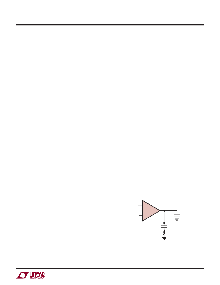
Optional Output Compensation for
Capacitive Loads Greater than 200pF
–
+
LT1638
VIN
1000pF
0.22μF
150Ω
Distortion
There are two main contributors of distortion in op amps:
output crossover distortion as the output transitions from
sourcing to sinking current and distortion caused by
相关PDF资料 |
PDF描述 |
|---|---|
| LTC2051HVHS8#PBF | IC OP-AMP ZERO-DRIFT DUAL 8-SOIC |
| 929836-01-09-RK | CONN HEADER 18POS DUAL .100 TIN |
| LT1884CS8#PBF | IC OP AMP DUAL R-R PICO/IN 8SOIC |
| ADA4000-4ARZ | IC OPAMP JFET 5MHZ QUAD 14SOIC |
| 9-103329-0-14 | CONN HEADR BRKWAY .100 14POS R/A |
相关代理商/技术参数 |
参数描述 |
|---|---|
| LT1638IMS8 | 制造商:Linear Technology 功能描述:OP Amp Dual GP R-R I/O ±22V/44V 8-Pin MSOP |
| LT1638IMS8#PBF | 功能描述:IC OPAMP R-R IN/OUT DUAL 8-MSOP RoHS:是 类别:集成电路 (IC) >> Linear - Amplifiers - Instrumentation 系列:Over-The-Top® 标准包装:100 系列:- 放大器类型:通用 电路数:1 输出类型:- 转换速率:0.2 V/µs 增益带宽积:- -3db带宽:- 电流 - 输入偏压:100pA 电压 - 输入偏移:30µV 电流 - 电源:380µA 电流 - 输出 / 通道:- 电压 - 电源,单路/双路(±):±2 V ~ 18 V 工作温度:0°C ~ 70°C 安装类型:表面贴装 封装/外壳:8-SOIC(0.154",3.90mm 宽) 供应商设备封装:8-SO 包装:管件 |
| LT1638IMS8#TR | 制造商:Linear Technology 功能描述:OP Amp Dual GP R-R I/O ±22V/44V 8-Pin MSOP T/R |
| LT1638IMS8#TRPBF | 功能描述:IC OPAMP R-R IN/OUT DUAL 8-MSOP RoHS:是 类别:集成电路 (IC) >> Linear - Amplifiers - Instrumentation 系列:Over-The-Top® 标准包装:100 系列:- 放大器类型:通用 电路数:1 输出类型:- 转换速率:0.2 V/µs 增益带宽积:- -3db带宽:- 电流 - 输入偏压:100pA 电压 - 输入偏移:30µV 电流 - 电源:380µA 电流 - 输出 / 通道:- 电压 - 电源,单路/双路(±):±2 V ~ 18 V 工作温度:0°C ~ 70°C 安装类型:表面贴装 封装/外壳:8-SOIC(0.154",3.90mm 宽) 供应商设备封装:8-SO 包装:管件 |
| LT1638IN8 | 功能描述:IC OPAMP R-R IN/OUT DUAL 8-DIP RoHS:否 类别:集成电路 (IC) >> Linear - Amplifiers - Instrumentation 系列:Over-The-Top® 标准包装:50 系列:LinCMOS™ 放大器类型:通用 电路数:4 输出类型:- 转换速率:0.05 V/µs 增益带宽积:110kHz -3db带宽:- 电流 - 输入偏压:0.7pA 电压 - 输入偏移:210µV 电流 - 电源:57µA 电流 - 输出 / 通道:30mA 电压 - 电源,单路/双路(±):3 V ~ 16 V,±1.5 V ~ 8 V 工作温度:-40°C ~ 85°C 安装类型:表面贴装 封装/外壳:14-SOIC(0.154",3.90mm 宽) 供应商设备封装:14-SOIC 包装:管件 产品目录页面:865 (CN2011-ZH PDF) 其它名称:296-1834296-1834-5 |
发布紧急采购,3分钟左右您将得到回复。