- 您现在的位置:买卖IC网 > PDF目录14072 > LT1676CS8 (Linear Technology)IC REG BUCK ADJ 0.7A 8SOIC PDF资料下载
参数资料
| 型号: | LT1676CS8 |
| 厂商: | Linear Technology |
| 文件页数: | 11/16页 |
| 文件大小: | 0K |
| 描述: | IC REG BUCK ADJ 0.7A 8SOIC |
| 标准包装: | 100 |
| 类型: | 降压(降压) |
| 输出类型: | 可调式 |
| 输出数: | 1 |
| 输出电压: | 1.24 V ~ 51 V |
| 输入电压: | 7.4 V ~ 60 V |
| PWM 型: | 电流模式,混合 |
| 频率 - 开关: | 100kHz |
| 电流 - 输出: | 700mA |
| 同步整流器: | 无 |
| 工作温度: | 0°C ~ 125°C |
| 安装类型: | 表面贴装 |
| 封装/外壳: | 8-SOIC(0.154",3.90mm 宽) |
| 包装: | 管件 |
| 供应商设备封装: | 8-SOIC |
�� �
�
�LT1676�
�APPLICATIO� N� S� I� N� FOR� M� ATIO� N�
�frequency� resonance� problems,� proper� layout� of� the� com-�
�ponents� connected� to� the� IC� is� essential,� especially� the�
�power� path.� B� field� (magnetic)� radiation� is� minimized� by�
�keeping� output� diode,� switch� pin� and� intput� bypass�
�capacitor� leads� as� short� as� possible.� E� field� radiation� is�
�kept� low� by� minimizing� the� length� and� area� of� all� traces�
�connected� to� the� switch� pin� (V� SW� ).� A� ground� plane� should�
�always� be� used� under� the� switcher� circuitry� to� prevent�
�interplane� coupling.�
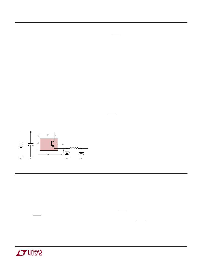
�The� high� speed� switching� current� path� is� shown� schemati-�
�cally� in� Figure� 3.� Minimum� lead� length� in� these� paths� is�
�essential� to� ensure� clean� switching� and� minimal� EMI.� The�
�paths� containing� the� input� capacitor,� output� switch� and�
�output� diode� are� the� only� ones� containing� nanosecond� rise�
�and� fall� times.� Keep� these� paths� as� short� as� possible.�
�Additionally,� it� is� possible� for� the� LT1676� to� cause� EMI�
�problems� by� “coupling� to� itself”.� Specifically,� this� can�
�occur� if� the� V� SW� pin� is� allowed� to� capacitively� couple� in� an�
�uncontrolled� manner� to� the� part’s� high� impedance� nodes,�
�i.e.,� SHDN,� SYNC,� V� C� and� FB.� This� can� cause� erratic�
�operation� such� as� odd/even� cycle� behavior,� pulse� width�
�“nervousness”,� improper� output� voltage� and/or� prema-�
�ture� current� limit� action.�
�As� an� example,� assume� that� the� capacitance� between� the�
�V� SW� node� and� a� high� impedance� pin� node� is� 0.1pF,� and�
�further� assume� that� the� high� impedance� node� in� question�
�exhibits� a� capacitance� of� 1pF� to� ground.� Due� to� the� high�
�dV/dt,� large� excursion� behavior� of� the� V� SW� node,� this� will�
�couple� a� nearly� 5V� transient� to� the� high� impedance� pin,�
�causing� abnormal� operation.� (This� assumes� the� “typical”�
�48V� IN� to� 5V� OUT� application.)� An� explicit� 100pF� capacitor�
�added� to� the� node� will� reduce� the� amplitude� of� the� distur-�
�bance� to� more� like� 50mV� (although� settling� time� will�
�increase).�
�Specific� pin� recommendations� are� as� follows:�
�SHDN:� If� unused,� add� a� 100pF� capacitor� to� ground.�
�SYNC:� Ground� if� unused.�
�V� C� :� Add� a� capacitor� directly� to� ground� in� addition� to� the�
�V� IN�
�+�
�C1�
�LT1676�
�V� IN�
�V� SW�
�D1�
�L1�
�+�
�C2�
�V� OUT�
�explicit� compensation� network.� A� value� of� one-tenth� of�
�the� main� compensation� capacitor� is� recommended,� up�
�to� a� maximum� of� 100pF.�
�FB:� Assuming� the� V� C� pin� is� handled� properly,� this� pin�
�usually� requires� no� explicit� capacitor� of� its� own,� but�
�1676� F03�
�Figure� 3.� High� Speed� Current� Switching� Paths�
�TYPICAL� APPLICATIO� N� S�
�Minimum� Component� Count� Application�
�Figure� 4a� shows� a� basic� “minimum� component� count”�
�application.� The� circuit� produces� 5V� at� up� to� 500mA� I� OUT�
�with� input� voltages� in� the� range� of� 12V� to� 48V.� The� typical�
�P� OUT� /P� IN� efficiency� is� shown� in� Figure� 4b.� No� pulse�
�skipping� is� observed� down� to� zero� external� load.� As�
�shown,� the� SHDN� and� SYNC� pins� are� unused,� however�
�either� (or� both)� can� be� optionally� driven� by� external� signals�
�as� desired.�
�keep� this� node� physically� small� to� minimize� stray� ca-�
�pacitance.�
�User� Programmable� Undervoltage� Lockout�
�Figure� 5� adds� a� resistor� divider� to� the� basic� application.�
�This� is� a� simple,� cost-effective� way� to� add� a� user-program-�
�mable� undervoltage� lockout� (UVLO)� function.� Resistor� R5�
�is� chosen� to� have� approximately� 200� μ� A� through� it� at� the�
�nominal� SHDN� pin� lockout� threshold� of� roughly� 1.25V.�
�The� somewhat� arbitrary� value� of� 200� μ� A� was� chosen� to� be�
�significantly� above� the� SHDN� pin� input� current� to� minimize�
�its� error� contribution,� but� significantly� below� the� typical�
�3.2mA� the� LT1676� draws� in� lockout� mode.� Resistor� R4� is�
�then� chosen� to� yield� this� same� 200� μ� A,� less� 2.5� μ� A,� with� the�
�11�
�相关PDF资料 |
PDF描述 |
|---|---|
| LT1111CS8-12#TRPBF | IC REG BUCK BOOST INV 12V 8SOIC |
| LT1111CS8-12#TR | IC REG BUCK BOOST INV 12V 8SOIC |
| LT1111CS8#TRPBF | IC REG BUCK BOOST INV ADJ 8SOIC |
| ECC25DRXS-S734 | CONN EDGECARD 50POS DIP .100 SLD |
| ESM30DTKI | CONN EDGECARD 60POS DIP .156 SLD |
相关代理商/技术参数 |
参数描述 |
|---|---|
| LT1676CS8#PBF | 功能描述:IC REG BUCK ADJ 0.7A 8SOIC RoHS:是 类别:集成电路 (IC) >> PMIC - 稳压器 - DC DC 开关稳压器 系列:- 标准包装:250 系列:- 类型:降压(降压) 输出类型:固定 输出数:1 输出电压:1.2V 输入电压:2.05 V ~ 6 V PWM 型:电压模式 频率 - 开关:2MHz 电流 - 输出:500mA 同步整流器:是 工作温度:-40°C ~ 85°C 安装类型:表面贴装 封装/外壳:6-UFDFN 包装:带卷 (TR) 供应商设备封装:6-SON(1.45x1) 产品目录页面:1032 (CN2011-ZH PDF) 其它名称:296-25628-2 |
| LT1676CS8#TR | 功能描述:IC REG BUCK ADJ 0.7A 8SOIC RoHS:否 类别:集成电路 (IC) >> PMIC - 稳压器 - DC DC 开关稳压器 系列:- 标准包装:2,500 系列:- 类型:升压(升压) 输出类型:可调式 输出数:1 输出电压:1.24 V ~ 30 V 输入电压:1.5 V ~ 12 V PWM 型:电流模式,混合 频率 - 开关:600kHz 电流 - 输出:500mA 同步整流器:无 工作温度:-40°C ~ 85°C 安装类型:表面贴装 封装/外壳:8-SOIC(0.154",3.90mm 宽) 包装:带卷 (TR) 供应商设备封装:8-SOIC |
| LT1676CS8#TRPBF | 功能描述:IC REG BUCK ADJ 0.7A 8SOIC RoHS:是 类别:集成电路 (IC) >> PMIC - 稳压器 - DC DC 开关稳压器 系列:- 标准包装:2,500 系列:- 类型:升压(升压) 输出类型:可调式 输出数:1 输出电压:1.24 V ~ 30 V 输入电压:1.5 V ~ 12 V PWM 型:电流模式,混合 频率 - 开关:600kHz 电流 - 输出:500mA 同步整流器:无 工作温度:-40°C ~ 85°C 安装类型:表面贴装 封装/外壳:8-SOIC(0.154",3.90mm 宽) 包装:带卷 (TR) 供应商设备封装:8-SOIC |
| LT1676CS8PBF | 制造商:Linear Technology 功能描述:Sw. Regulator Step-Down 7.4-60V SOIC8 |
| LT1676I | 制造商:LINER 制造商全称:Linear Technology 功能描述:Wide Input Range, High Efficiency, Step-Down Switching Regulator |
发布紧急采购,3分钟左右您将得到回复。