- 您现在的位置:买卖IC网 > PDF目录2083 > LT1712IGN#TRPBF (Linear Technology)IC COMP R-R I/O DUAL LP 16SSOP PDF资料下载
参数资料
| 型号: | LT1712IGN#TRPBF |
| 厂商: | Linear Technology |
| 文件页数: | 11/12页 |
| 文件大小: | 0K |
| 描述: | IC COMP R-R I/O DUAL LP 16SSOP |
| 标准包装: | 2,500 |
| 系列: | UltraFast™ |
| 类型: | 带锁销 |
| 元件数: | 2 |
| 输出类型: | CMOS,补充型,满摆幅,TTL |
| 电压 - 电源,单路/双路(±): | 2.4 V ~ 12 V,±2.4 V ~ 6 V |
| 电压 - 输入偏移(最小值): | 5mV @ 5V |
| 电流 - 输入偏压(最小值): | 5µA @ 5V |
| 电流 - 输出(标准): | 20mA |
| 电流 - 静态(最大值): | 22mA |
| CMRR, PSRR(标准): | 75dB CMRR,85dB PSRR |
| 传输延迟(最大): | 6ns |
| 磁滞: | 100mV |
| 工作温度: | -40°C ~ 85°C |
| 封装/外壳: | 16-SSOP(0.154",3.90mm 宽) |
| 安装类型: | 表面贴装 |
| 包装: | 带卷 (TR) |
8
LT1711/LT1712
latch when a flow-through condition is desired. The latch
pin is designed to be driven with either a TTL or CMOS
output. It has built-in hysteresis of approximately 100mV,
so that slow moving or noisy input signals do not impact
latch performance.
For the LT1712, if only one of the comparators is being
used at a given time, it is best to latch the second compara-
tor to avoid any possibility of interactions between the two
comparators in the same package.
High Speed Design Techniques
The extremely fast speed of the LT1711/LT1712 necessi-
tates careful attention to proper PC board layout and
circuit design in order to prevent oscillations, as with
most high speed comparators. The most common prob-
lem involves power supply bypassing which is necessary
to maintain low supply impedance. Resistance and induc-
tance in supply wires and PC traces can quickly build up
to unacceptable levels, thereby allowing the supply volt-
ages to move as the supply current changes. This move-
ment of the supply voltages will often result in improper
operation. In addition, adjacent devices connected through
an unbypassed supply can interact with each other through
the finite supply impedances.
Bypass capacitors furnish a simple solution to this prob-
lem by providing a local reservoir of energy at the device,
thus keeping supply impedance low. Bypass capacitors
should be as close as possible to the LT1711/LT1712
supply pins. A good high frequency capacitor, such as a
1000pF ceramic, is recommended in parallel with larger
capacitors, such as a 0.1
F ceramic and a 4.7F tantalum
in parallel. These bypass capacitors should be soldered to
the output ground plane such that the return currents do
not pass through the ground plane under the input cir-
cuitry. The common tie point for these two ground planes
should be at the board ground connection. Such star-
grounding and ground plane separation is extremely im-
portant for the proper operation of ultra high speed circuits.
Poor trace routes and high source impedances are also
common sources of problems. Keep trace lengths as short
as possible and avoid running any output trace adjacent
to an input trace to prevent unnecessary coupling. If
output traces are longer than a few inches, provide proper
termination impedances (typically 100
to 400) to
eliminate any reflections that may occur. Also keep source
impedances as low as possible, preferably much less than
1k
.
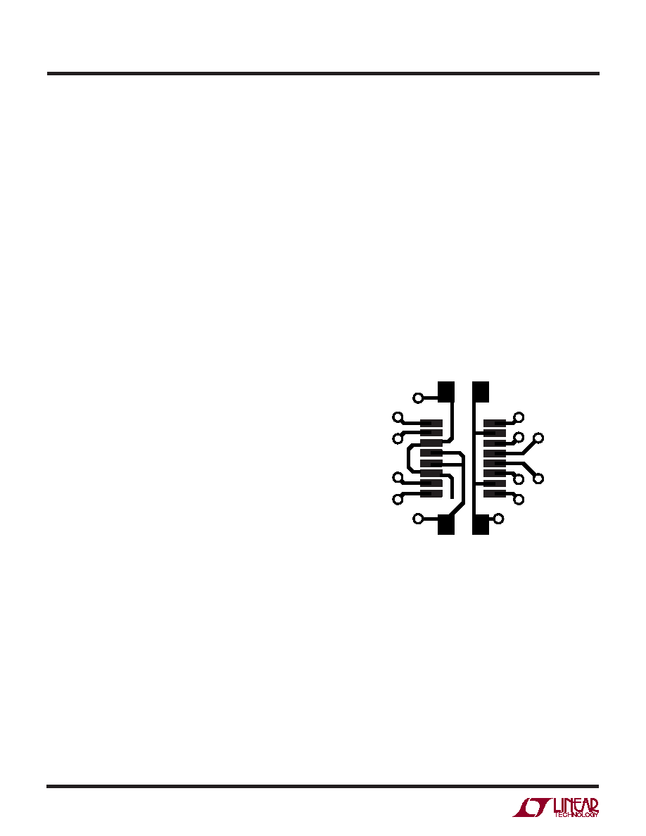
The input and output traces should also be isolated from
one another. Power supply traces can be used to achieve
this isolation as shown in Figure 1, a typical topside layout
of the LT1712 on a multilayer PC board. Shown is the
topside metal etch including traces, pin escape vias and
the land pads for a GN16 LT1712 and its adjacent X7R
0805 bypass capacitors. The V+, V– and GND traces all
shield the inputs from the outputs. Although the two V–
pins are connected internally, they should be shorted
together externally as well in order for both to function as
shields. The same is true for the two V+ pins. The two GND
pins are not connected internally, but in most applications
they are both connected directly to the ground plane.
APPLICATIO S I FOR ATIO
WU
UU
171112 F01
Figure 1. Typical LT1712 Topside Metal
for Multilayer PCB Layout
Hysteresis
Another important technique to avoid oscillations is to
provide positive feedback, also known as hysteresis,
from the output to the input. Increased levels of hyster-
esis, however, reduce the sensitivity of the device to input
voltage levels, so the amount of positive feedback should
be tailored to particular system requirements. The
LT1711/LT1712 are completely flexible regarding the
application of hysteresis, due to rail-to-rail inputs and the
complementary outputs. Specifically, feedback resistors
can be connected from one of the outputs to its corre-
sponding input without regard to common mode consid-
erations. Figure 2 shows several configurations.
相关PDF资料 |
PDF描述 |
|---|---|
| LT1714IGN#TR | IC COMP R-R I/O DUAL LP 16SSOP |
| LT1715HMS#TRPBF | IC COMPARATOR 4NS DUAL 10-MSOP |
| LT1716IS5#TRPBF | IC COMP OTT R-R 44V TSOT-23-5 |
| LT1719IS8#TRPBF | IC COMP R-RINOUT SINGLE 8-SOIC |
| LT1721IGN#TRPBF | IC COMP R-RINOUT QUAD 16-SSOP |
相关代理商/技术参数 |
参数描述 |
|---|---|
| LT1713 | 制造商:未知厂家 制造商全称:未知厂家 功能描述:UNDERSTANDING THE SUBJECT IS CUSTOMER SERVICE |
| LT1713CMS8 | 功能描述:IC COMP R-R I/O SINGLE LP 8MSOP RoHS:否 类别:集成电路 (IC) >> 线性 - 比较器 系列:UltraFast™ 标准包装:25 系列:- 类型:带电压基准 元件数:4 输出类型:CMOS,开路漏极,TTL 电压 - 电源,单路/双路(±):2 V ~ 11 V,±1 V ~ 5.5 V 电压 - 输入偏移(最小值):10mV @ 5V 电流 - 输入偏压(最小值):- 电流 - 输出(标准):0.015mA @ 5V 电流 - 静态(最大值):8.5µA CMRR, PSRR(标准):80dB CMRR,80dB PSRR 传输延迟(最大):12µs 磁滞:50mV 工作温度:0°C ~ 70°C 封装/外壳:16-DIP(0.300",7.62mm) 安装类型:通孔 包装:管件 |
| LT1713CMS8#PBF | 功能描述:IC COMP R-R I/O SINGLE LP 8MSOP RoHS:是 类别:集成电路 (IC) >> 线性 - 比较器 系列:UltraFast™ 标准包装:1 系列:- 类型:通用 元件数:1 输出类型:CMOS,开路集电极,TTL 电压 - 电源,单路/双路(±):2.7 V ~ 5.5 V 电压 - 输入偏移(最小值):7mV @ 5V 电流 - 输入偏压(最小值):0.25µA @ 5V 电流 - 输出(标准):84mA @ 5V 电流 - 静态(最大值):120µA CMRR, PSRR(标准):- 传输延迟(最大):600ns 磁滞:- 工作温度:-40°C ~ 85°C 封装/外壳:SC-74A,SOT-753 安装类型:表面贴装 包装:剪切带 (CT) 产品目录页面:1268 (CN2011-ZH PDF) 其它名称:*LMV331M5*LMV331M5/NOPBLMV331M5CT |
| LT1713CMS8#TR | 功能描述:IC COMP R-R I/O SINGLE LP 8MSOP RoHS:否 类别:集成电路 (IC) >> 线性 - 比较器 系列:UltraFast™ 标准包装:25 系列:- 类型:带电压基准 元件数:4 输出类型:CMOS,开路漏极,TTL 电压 - 电源,单路/双路(±):2 V ~ 11 V,±1 V ~ 5.5 V 电压 - 输入偏移(最小值):10mV @ 5V 电流 - 输入偏压(最小值):- 电流 - 输出(标准):0.015mA @ 5V 电流 - 静态(最大值):8.5µA CMRR, PSRR(标准):80dB CMRR,80dB PSRR 传输延迟(最大):12µs 磁滞:50mV 工作温度:0°C ~ 70°C 封装/外壳:16-DIP(0.300",7.62mm) 安装类型:通孔 包装:管件 |
| LT1713CMS8#TRPBF | 功能描述:IC COMP R-R I/O SINGLE LP 8MSOP RoHS:是 类别:集成电路 (IC) >> 线性 - 比较器 系列:UltraFast™ 标准包装:25 系列:- 类型:带电压基准 元件数:4 输出类型:CMOS,开路漏极,TTL 电压 - 电源,单路/双路(±):2 V ~ 11 V,±1 V ~ 5.5 V 电压 - 输入偏移(最小值):10mV @ 5V 电流 - 输入偏压(最小值):- 电流 - 输出(标准):0.015mA @ 5V 电流 - 静态(最大值):8.5µA CMRR, PSRR(标准):80dB CMRR,80dB PSRR 传输延迟(最大):12µs 磁滞:50mV 工作温度:0°C ~ 70°C 封装/外壳:16-DIP(0.300",7.62mm) 安装类型:通孔 包装:管件 |
发布紧急采购,3分钟左右您将得到回复。