- 您现在的位置:买卖IC网 > PDF目录2083 > LT1715HMS#TRPBF (Linear Technology)IC COMPARATOR 4NS DUAL 10-MSOP PDF资料下载
参数资料
| 型号: | LT1715HMS#TRPBF |
| 厂商: | Linear Technology |
| 文件页数: | 5/20页 |
| 文件大小: | 0K |
| 描述: | IC COMPARATOR 4NS DUAL 10-MSOP |
| 标准包装: | 2,500 |
| 系列: | UltraFast™ |
| 类型: | 通用 |
| 元件数: | 2 |
| 输出类型: | CMOS,满摆幅,TTL |
| 电压 - 电源,单路/双路(±): | 2.7 V ~ 12 V |
| 电压 - 输入偏移(最小值): | 2.5mV @ ±5V |
| 电流 - 输入偏压(最小值): | 7µA @ ±5V |
| 电流 - 输出(标准): | 20mA |
| 电流 - 静态(最大值): | 2.2mA |
| CMRR, PSRR(标准): | 55dB CMRR,80dB PSRR |
| 传输延迟(最大): | 9ns |
| 磁滞: | 7mV |
| 工作温度: | -40°C ~ 125°C |
| 封装/外壳: | 10-TFSOP,10-MSOP(0.118",3.00mm 宽) |
| 安装类型: | 表面贴装 |
| 包装: | 带卷 (TR) |
LT1715
13
1715fa
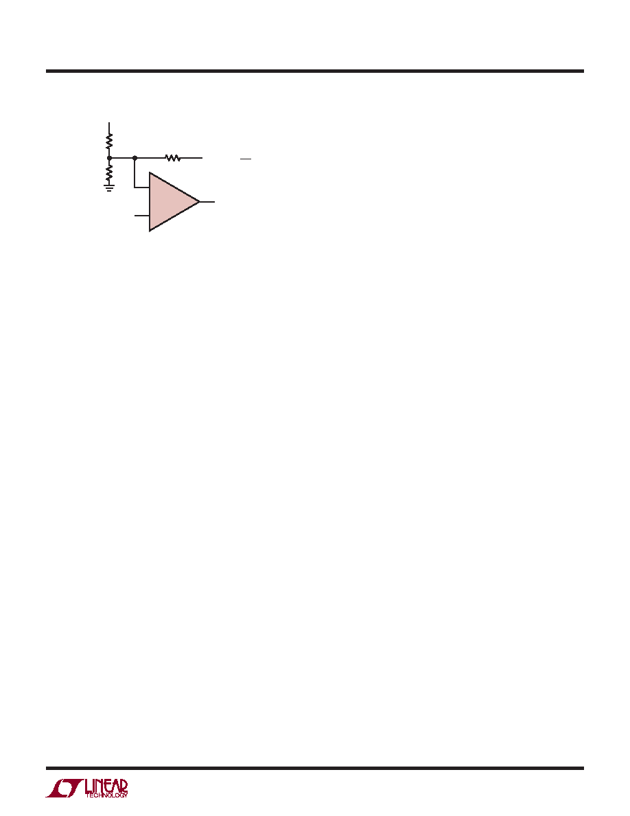
The second step is to recalculate R2 to set the same av-
erage threshold as before. The average threshold before
was set at VTH = (VREF)(R1)/(R1 + R2). The new R2 is
calculated based on the average output voltage (+VS/2)and
the simplied circuit model in Figure 7. To assure that the
comparator’s noninverting input is, on average, the same
VTH as before:
R2 = (VREF – VTH)/(VTH/R1 + (VTH – VS/2)/R3)
For additional hysteresis of 10mV or less, it is not uncom-
mon for R2 to be the same as R2 within 1% resistor
tolerances.
This method will work for additional hysteresis of up to
a few hundred millivolts. Beyond that, the impedance of
R3 is low enough to effect the bias string, and adjust-
ment of R1 may also be required. Note that the currents
through the R1/R2 bias string should be many times the
input currents of the LT1715. For 5% accuracy, the cur-
rent must be at least 20 times the input current, more for
higher accuracy.
Interfacing the LT1715 to ECL
The LT1715’s comparators can be used in high speed ap-
plications where Emitter-Coupled Logic (ECL) is deployed.
To interface the output of the LT1715 to ECL logic inputs,
standard TTL/CMOS to ECL level translators such as the
10H124, 10H424 and 100124 can be used. The secom-
ponents come at a cost of a few nanoseconds additional
delay as well as supply currents of 50mA or more, and
are only available in quads. A faster, simpler and lower
power translator can be constructed with resistors as
shown in Figure 8.
Figure 8a shows the standard TTL to Positive ECL (PECL)
resistive level translator. This translator cannot be used
forthe LT1715, or with CMOS logic, because it depends
on the 820Ω resistor to limit the output swing (VOH) of
the all-NPNTTL gate with its so-called totem-pole output.
The LT1715is fabricated in a complementary bipolar
process and the output stage has a PNP driver that pulls
the output nearly all the way to the supply rail, even when
sourcing 10mA.
Figure 8b shows a three resistor level translator for inter-
facing the LT1715 to ECL running off the same supply rail.
No pull-down on the output of the LT1715 is needed, but
pull-down R3 limits the VIH seen by the PECL gate. This
is needed because ECL inputs have both a minimum and
maximum VIH specication for proper operation. Resis-
tor values are given for both ECL interface types; in both
cases it is assumed that the LT1715 operates from the
same supply rail.
Figure 8c shows the case of translating to PECL from
an LT1715 powered by a 3V supply rail. Again, resistor
values are given for both ECL interface types. This time
four resistors are needed, although with 10KH/E, R3 is not
needed. In that case, the circuit resembles the standard
TTL translator of Figure 8a, but the function of the new
resistor, R4, is much different. R4 loads the LT1715 output
when high so that the current owing through R1 doesn’t
forward bias the LT1715’s internal ESD clamp diode.
Although this diode can handle 20mA without damage,
normal operation and performance of the output stage can
be impaired above 100μA of forward current. R4 prevents
this with the minimum additional power dissipation.
Finally, Figure 8d shows the case of driving standard,
negative-rail, ECL with the LT1715. Resistor values are
given for both ECL interface types and for both a 5V
and 3V LT1715 supply rail. Again, a fourth resistor, R4
is needed to prevent the low state current from owing
out of the LT1715, turning on the internal ESD/substrate
diodes. Resistor R4 again prevents this with the minimum
additional power dissipation.
APPLICATIONS INFORMATION
Figure 7. Model for Additional Hysteresis Calculations
–
+
1/2 LT1715
1715 F07
R2
VREF
VTH
R3
+VS
2
VAVERAGE =
R1
相关PDF资料 |
PDF描述 |
|---|---|
| LT1716IS5#TRPBF | IC COMP OTT R-R 44V TSOT-23-5 |
| LT1719IS8#TRPBF | IC COMP R-RINOUT SINGLE 8-SOIC |
| LT1721IGN#TRPBF | IC COMP R-RINOUT QUAD 16-SSOP |
| LT319AN | IC COMPARATOR DUAL 14-DIP |
| LT3469ETS8#TRMPBF | IC AMP DVR W/REG 1.3MHZ TSOT23-8 |
相关代理商/技术参数 |
参数描述 |
|---|---|
| LT1715IMS | 功能描述:IC COMPARATOR 150MHZ DUAL 10MSOP RoHS:否 类别:集成电路 (IC) >> 线性 - 比较器 系列:UltraFast™ 产品培训模块:Lead (SnPb) Finish for COTS Obsolescence Mitigation Program 标准包装:2,500 系列:- 类型:通用 元件数:1 输出类型:CMOS,推挽式,满摆幅,TTL 电压 - 电源,单路/双路(±):2.5 V ~ 5.5 V,±1.25 V ~ 2.75 V 电压 - 输入偏移(最小值):5mV @ 5.5V 电流 - 输入偏压(最小值):1pA @ 5.5V 电流 - 输出(标准):- 电流 - 静态(最大值):24µA CMRR, PSRR(标准):80dB CMRR,80dB PSRR 传输延迟(最大):450ns 磁滞:±3mV 工作温度:-40°C ~ 85°C 封装/外壳:6-WFBGA,CSPBGA 安装类型:表面贴装 包装:管件 其它名称:Q3554586 |
| LT1715IMS#PBF | 功能描述:IC COMPARATOR 150MHZ DUAL 10MSOP RoHS:是 类别:集成电路 (IC) >> 线性 - 比较器 系列:UltraFast™ 产品培训模块:Lead (SnPb) Finish for COTS Obsolescence Mitigation Program 标准包装:2,500 系列:- 类型:通用 元件数:1 输出类型:CMOS,推挽式,满摆幅,TTL 电压 - 电源,单路/双路(±):2.5 V ~ 5.5 V,±1.25 V ~ 2.75 V 电压 - 输入偏移(最小值):5mV @ 5.5V 电流 - 输入偏压(最小值):1pA @ 5.5V 电流 - 输出(标准):- 电流 - 静态(最大值):24µA CMRR, PSRR(标准):80dB CMRR,80dB PSRR 传输延迟(最大):450ns 磁滞:±3mV 工作温度:-40°C ~ 85°C 封装/外壳:6-WFBGA,CSPBGA 安装类型:表面贴装 包装:管件 其它名称:Q3554586 |
| LT1715IMS#PBF | 制造商:Linear Technology 功能描述:COMPARATOR DUAL 4NS MSOP-10 制造商:Linear Technology 功能描述:COMPARATOR, DUAL, 4NS, MSOP-10 |
| LT1715IMS#TR | 功能描述:IC COMPARATOR 150MHZ DUAL 10MSOP RoHS:否 类别:集成电路 (IC) >> 线性 - 比较器 系列:UltraFast™ 产品培训模块:Lead (SnPb) Finish for COTS Obsolescence Mitigation Program 标准包装:2,500 系列:- 类型:通用 元件数:1 输出类型:CMOS,推挽式,满摆幅,TTL 电压 - 电源,单路/双路(±):2.5 V ~ 5.5 V,±1.25 V ~ 2.75 V 电压 - 输入偏移(最小值):5mV @ 5.5V 电流 - 输入偏压(最小值):1pA @ 5.5V 电流 - 输出(标准):- 电流 - 静态(最大值):24µA CMRR, PSRR(标准):80dB CMRR,80dB PSRR 传输延迟(最大):450ns 磁滞:±3mV 工作温度:-40°C ~ 85°C 封装/外壳:6-WFBGA,CSPBGA 安装类型:表面贴装 包装:管件 其它名称:Q3554586 |
| LT1715IMS#TRPBF | 功能描述:IC COMPARATOR 150MHZ DUAL 10MSOP RoHS:是 类别:集成电路 (IC) >> 线性 - 比较器 系列:UltraFast™ 产品培训模块:Lead (SnPb) Finish for COTS Obsolescence Mitigation Program 标准包装:2,500 系列:- 类型:通用 元件数:1 输出类型:CMOS,推挽式,满摆幅,TTL 电压 - 电源,单路/双路(±):2.5 V ~ 5.5 V,±1.25 V ~ 2.75 V 电压 - 输入偏移(最小值):5mV @ 5.5V 电流 - 输入偏压(最小值):1pA @ 5.5V 电流 - 输出(标准):- 电流 - 静态(最大值):24µA CMRR, PSRR(标准):80dB CMRR,80dB PSRR 传输延迟(最大):450ns 磁滞:±3mV 工作温度:-40°C ~ 85°C 封装/外壳:6-WFBGA,CSPBGA 安装类型:表面贴装 包装:管件 其它名称:Q3554586 |
发布紧急采购,3分钟左右您将得到回复。