- 您现在的位置:买卖IC网 > PDF目录10681 > LT1715IMS#TR (Linear Technology)IC COMPARATOR 150MHZ DUAL 10MSOP PDF资料下载
参数资料
| 型号: | LT1715IMS#TR |
| 厂商: | Linear Technology |
| 文件页数: | 15/20页 |
| 文件大小: | 0K |
| 描述: | IC COMPARATOR 150MHZ DUAL 10MSOP |
| 标准包装: | 2,500 |
| 系列: | UltraFast™ |
| 类型: | 通用 |
| 元件数: | 2 |
| 输出类型: | CMOS,满摆幅,TTL |
| 电压 - 电源,单路/双路(±): | 2.7 V ~ 12 V |
| 电压 - 输入偏移(最小值): | 2.5mV @ ±5V |
| 电流 - 输入偏压(最小值): | 6µA @ ±5V |
| 电流 - 输出(标准): | 20mA |
| 电流 - 静态(最大值): | 2mA |
| CMRR, PSRR(标准): | 70dB CMRR,80dB PSRR |
| 传输延迟(最大): | 9ns |
| 磁滞: | 6mV |
| 工作温度: | -40°C ~ 85°C |
| 封装/外壳: | 10-TFSOP,10-MSOP(0.118",3.00mm 宽) |
| 安装类型: | 表面贴装 |
| 包装: | 带卷 (TR) |
| 其它名称: | LT1715IMSTR |
LT1715
4
1715fa
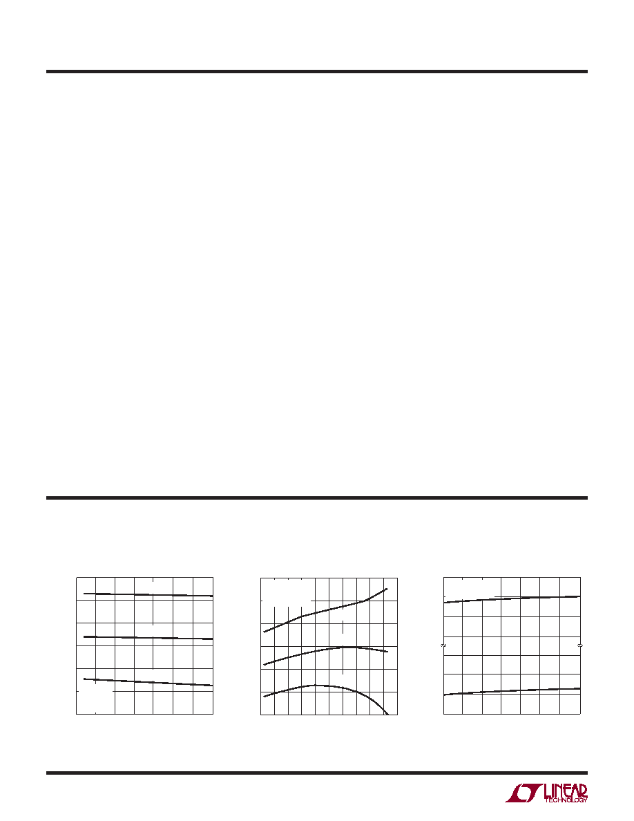
ELECTRICAL CHARACTERISTICS
Input Offset and Trip Voltages
vs Supply Voltage
Input Offset and Trip Voltages
vs Temperature
Input Common Mode Limits
vs Temperature
SUPPLY VOLTAGE, VCC = +VS (V)
2.5
V
OS
AND
TRIP
POINT
VOLTAGE
(mV)
3
2
1
0
–1
–2
–3
4.0
5.0
1715 G01
3.0
3.5
4.5
5.5
6.0
VTRIP
+
VOS
VTRIP
–
TA = 25°C
VCM = 1V
VEE = GND
TEMPERATURE (°C)
–3
V
OS
AND
TRIP
POINT
VOLTAGE
(mV)
–1
1
3
–2
0
2
–20
20
60
100
1715 G02
140
–40
–60
0
40
80
120
VTRIP
+
VOS
VTRIP
–
+VS = VCC = 5V
VCM = 1V
VEE = –5V
TEMPERATURE (°C)
–50
3.6
3.8
4.2
25
75
1715 G03
–4.8
–5.0
–25
0
50
100
125
–5.2
–5.4
4.0
COMMON
MODE
INPUT
VOLTAGE
(V)
+VS = VCC = 5V
VEE = –5V
Note 1: Stresses beyond those listed under Absolute Maximum Ratings
may cause permanent damage to the device. Exposure to any Absolute
Maximum Rating condition for extended periods may affect device
reliability and lifetime.
Note 2: The LT1715C is guaranteed functional over the operating range of
–40°C to 85°C.
Note 3: The LT1715C is guaranteed to meet specied performance from
0°C to 70°C. The LT1715°C is designed, characterized and expected to
meet specied performance from –40°C to 85°C but is not tested or
QA sampled at these temperatures. The LT1715I is guaranteed to meet
specied performance from –40°C to 85°C. The LT1715H is guaranteed to
meet specied performance from –40°C to 125°C.
Note 4: Thermal resistances vary depending upon the amount of PC board
metal attached to Pin 5 of the device. θJA is specied for a 2500mm2 3/32"
FR-4 board covered with 2oz copper on both sides and with 100mm2 of
copper attached to Pin 5. Thermal performance can be improved beyond
the given specication by using a 4-layer board or by attaching more metal
area to Pin 5.
Note 5: If one input is within these common mode limits, the other input
can go outside the common mode limits and the output will be valid.
Note 6: The LT1715 comparator includes internal hysteresis. The trip
points are the input voltage needed to change the output state in each
direction. The offset voltage is dened as the average of VTRIP+ and VTRIP–,
while the hysteresis voltage is the difference of these two.
Note 7: The common mode rejection ratio is measured with VCC = 5V,
VEE = –5V and is dened as the change in offset voltage measured from
VCM = –5.1V to VCM = 3.8V, divided by 8.9V.
Note 8: The power supply rejection ratio is measured with VCM = 1V and is
dened as the worst of: the change in offset voltage from VCC = +VS = 2.7V
to VCC = +VS = 6V (with VEE = 0V) divided by 3.3V or the change in offset
voltage from VEE = 0V to VEE = –6V (with VCC = +VS = 6V) divided by 6V.
Note 9: Because of internal hysteresis, there is no small-signal region in
which to measure gain. Proper operation of internal circuity is ensured by
measuring VOH and VOL with only 20mV of overdrive.
Note 10: Maximum toggle rate is dened as the highest frequency at
which a 100mV sinusoidal input results in an error free output toggling to
greater than 4V when high and to less than 1V when low on a 5V output
supply.
Note 11: Propagation delay measurements made with 100mV steps.
Overdrive is measured relative to VTRIP±.
Note 12: tPD cannot be measured in automatic handling equipment with
low values of overdrive. The LT1715 is 100% tested with a 100mV step
and 20mV overdrive. Correlation tests have shown that tPD limits can be
guaranteed with this test.
Note 13: Propagation Delay Skew is dened as:
tSKEW = |tPDLH – tPDHL|
Note 14: Differential propagation delay is dened as the larger of the two:
ΔtPDLH = |tPDLHA – tPDLHB|
ΔtPDHL = |tPDHLA – tPDHLB|
Note 15: Package inductances combined with asynchronous activity on
the other channel can increase the output jitter. See Channel Interactions
in Applications Information. Specication above is with one channel active
only.
TYPICAL PERFORMANCE CHARACTERISTICS
相关PDF资料 |
PDF描述 |
|---|---|
| AD8612ARUZ-REEL | IC COMP DUAL 4NS FAST 14-TSSOP |
| AD9609BCPZ-40 | IC ADC 10BIT 40MSPS LP 32LFCSP |
| AD7276BUJZ-500RL7 | IC ADC 12BIT 3MSPS TSOT23-6 |
| LT1720IMS8#PBF | IC COMPARATOR DUAL HS 3/5V 8MSOP |
| LT1720IMS8 | IC COMPARATOR DUAL HS 3/5V 8MSOP |
相关代理商/技术参数 |
参数描述 |
|---|---|
| LT1715IMSTRPBF | 制造商:LINER 制造商全称:Linear Technology 功能描述:4ns, 150MHz Dual Comparator with Independent Input/Output Supplies |
| LT1716 | 制造商:LINER 制造商全称:Linear Technology 功能描述:SOT-23, 44V, Over-The-Top, Micropower, Precision Rail-to-Rail Comparator |
| LT1716CS5 | 制造商:Linear Technology 功能描述:Comparator Single R-R O/P ±22V/44V 5-Pin TSOT-23 |
| LT1716CS5#PBF | 制造商:Linear Technology 功能描述:COMPARATOR PRECISION R/R SOT-23-5 制造商:Linear Technology 功能描述:COMPARATOR PRECISION SINGLE 制造商:Linear Technology 功能描述:COMPARATOR, PRECISION R/R, SOT-23-5 制造商:Linear Technology 功能描述:COMPARATOR, PRECISION, SINGLE, TSOT-23-5; Comparator Type:Precision; No. of Comparators:1; Response Time:3s; Supply Voltage Range:2.7V to 44V; Amplifier Case Style:TSOT-23; No. of Pins:5; IC Output Type:Pull Up; Supply Current:40A ;RoHS Compliant: Yes |
| LT1716CS5#TR | 功能描述:IC COMP OTT R-R 44V TSOT-23-5 RoHS:否 类别:集成电路 (IC) >> 线性 - 比较器 系列:Over-The-Top® 标准包装:25 系列:- 类型:带电压基准 元件数:4 输出类型:CMOS,开路漏极,TTL 电压 - 电源,单路/双路(±):2 V ~ 11 V,±1 V ~ 5.5 V 电压 - 输入偏移(最小值):10mV @ 5V 电流 - 输入偏压(最小值):- 电流 - 输出(标准):0.015mA @ 5V 电流 - 静态(最大值):8.5µA CMRR, PSRR(标准):80dB CMRR,80dB PSRR 传输延迟(最大):12µs 磁滞:50mV 工作温度:0°C ~ 70°C 封装/外壳:16-DIP(0.300",7.62mm) 安装类型:通孔 包装:管件 |
发布紧急采购,3分钟左右您将得到回复。