- 您现在的位置:买卖IC网 > PDF目录10681 > LT1715IMS#TRPBF (Linear Technology)IC COMPARATOR 150MHZ DUAL 10MSOP PDF资料下载
参数资料
| 型号: | LT1715IMS#TRPBF |
| 厂商: | Linear Technology |
| 文件页数: | 2/20页 |
| 文件大小: | 0K |
| 描述: | IC COMPARATOR 150MHZ DUAL 10MSOP |
| 标准包装: | 2,500 |
| 系列: | UltraFast™ |
| 类型: | 通用 |
| 元件数: | 2 |
| 输出类型: | CMOS,满摆幅,TTL |
| 电压 - 电源,单路/双路(±): | 2.7 V ~ 12 V |
| 电压 - 输入偏移(最小值): | 2.5mV @ ±5V |
| 电流 - 输入偏压(最小值): | 6µA @ ±5V |
| 电流 - 输出(标准): | 20mA |
| 电流 - 静态(最大值): | 2mA |
| CMRR, PSRR(标准): | 70dB CMRR,80dB PSRR |
| 传输延迟(最大): | 9ns |
| 磁滞: | 6mV |
| 工作温度: | -40°C ~ 85°C |
| 封装/外壳: | 10-TFSOP,10-MSOP(0.118",3.00mm 宽) |
| 安装类型: | 表面贴装 |
| 包装: | 带卷 (TR) |
LT1715
10
1715fa
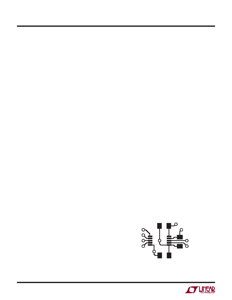
Figure 2. Typical Topside Metal for Multilayer PCB Layouts
1715 F02
APPLICATIONS INFORMATION
When both input signals are above the positive common
mode limit, the input stage will get debiased and the output
polarity will be random. However, the internal hysteresis
will hold the output to a valid logic level. When at least one
of the inputs returns to within the common mode limits,
recovery from this state will take as long as 1μs.
The propagation delay does not increase signicantly when
driven with large differential voltages, but with low levels
of overdrive, an apparent increase may be seen with large
source resistances due to an RC delay caused by the 2pF
typical input capacitance.
Input Protection
The input stage is protected against damage from large
differential signals, up to and beyond a differential voltage
equal to the supply voltage, limited only by the absolute
maximum currents noted. External input protection cir-
cuitry is only needed if currents would otherwise exceed
these absolute maximums. The internal catch diodes can
conduct current up to these rated maximums without
latchup, even when the supply voltages are at the absolute
maximum ratings.
The LT1715 input stage has general purpose internal ESD
protection for the human body model. For use as a line
receiver, additional external protection may be required.
As with most integrated circuits, the level of immunity to
ESD is much greater when residing on a printed circuit
board where the power supply decoupling capacitance will
limit the voltage rise caused by an ESD pulse.
Input Bias Current
Input bias current is measured with both inputs held at
1V. As with any PNP differential input stage, the LT1715
bias current ows out of the device. It will go to zero on
the higher of the two inputs and double on the lower
of the two inputs. With more than two diode drops of
differential input voltage, the LT1715’s input protection
circuitry activates, and current out of the lower input will
increase an additional 30% and there will be a small bias
current into the higher of the two input pins, of 4μA or
less. See the Typical Performance curve “Input Current
vs Differential Input Voltage.”
High Speed Design Considerations
Application of high speed comparators is often plagued by
oscillations. The LT1715 has 4mV of internal hysteresis,
which will prevent oscillations as long as parasitic output
to input feedback is kept below 4mV. However, with the
2V/ns slew rate of the LT1715 outputs, a 4mV step can
be created at a 100Ω input source with only 0.02pF of
output to input coupling. The LT1715’s pinout has been
arranged to minimize problems by placing the sensitive
inputs away from the outputs, shielded by the power rails.
The input and output traces of the circuit board should
also be separated, and the requisite level of isolation is
readily achieved if a topside ground plane runs between
the output and the inputs. For multilayer boards where the
ground plane is internal, a topside ground or supply trace
should be run between the inputs and the output.
The ground pin of the LT1715 can disturb the ground plane
potential while toggling due to the extremely fast on and
off times of the output stage. Therefore, using a ground
for input termination or ltering that is separate from the
LT1715 Pin 6 ground can be highly benecial. For example,
a ground plane tied to Pin 6 and directly adjacent to a 1"
long input trace can capacitively couple 4mV of disturbance
into the input. In this scenario, cutting the ground plane
between the GND pin and the inputs will cut the capacitance
and the disturbance down substantially.
Figure 2 shows a typical topside layout of the LT1715
on such a multilayer board. Shown is the topside metal
etch including traces, pin escape vias, and the land pads
for an MS10 LT1715 and its adjacent X7R 10nF bypass
capacitors in the 0805 case.
相关PDF资料 |
PDF描述 |
|---|---|
| CS5525-ASZ | IC ADC 16BIT W/4BIT LATCH 20SSOP |
| LT1715IMS#TR | IC COMPARATOR 150MHZ DUAL 10MSOP |
| AD8612ARUZ-REEL | IC COMP DUAL 4NS FAST 14-TSSOP |
| AD9609BCPZ-40 | IC ADC 10BIT 40MSPS LP 32LFCSP |
| AD7276BUJZ-500RL7 | IC ADC 12BIT 3MSPS TSOT23-6 |
相关代理商/技术参数 |
参数描述 |
|---|---|
| LT1716 | 制造商:LINER 制造商全称:Linear Technology 功能描述:SOT-23, 44V, Over-The-Top, Micropower, Precision Rail-to-Rail Comparator |
| LT1716CS5 | 制造商:Linear Technology 功能描述:Comparator Single R-R O/P ±22V/44V 5-Pin TSOT-23 |
| LT1716CS5#PBF | 制造商:Linear Technology 功能描述:COMPARATOR PRECISION R/R SOT-23-5 制造商:Linear Technology 功能描述:COMPARATOR PRECISION SINGLE 制造商:Linear Technology 功能描述:COMPARATOR, PRECISION R/R, SOT-23-5 制造商:Linear Technology 功能描述:COMPARATOR, PRECISION, SINGLE, TSOT-23-5; Comparator Type:Precision; No. of Comparators:1; Response Time:3s; Supply Voltage Range:2.7V to 44V; Amplifier Case Style:TSOT-23; No. of Pins:5; IC Output Type:Pull Up; Supply Current:40A ;RoHS Compliant: Yes |
| LT1716CS5#TR | 功能描述:IC COMP OTT R-R 44V TSOT-23-5 RoHS:否 类别:集成电路 (IC) >> 线性 - 比较器 系列:Over-The-Top® 标准包装:25 系列:- 类型:带电压基准 元件数:4 输出类型:CMOS,开路漏极,TTL 电压 - 电源,单路/双路(±):2 V ~ 11 V,±1 V ~ 5.5 V 电压 - 输入偏移(最小值):10mV @ 5V 电流 - 输入偏压(最小值):- 电流 - 输出(标准):0.015mA @ 5V 电流 - 静态(最大值):8.5µA CMRR, PSRR(标准):80dB CMRR,80dB PSRR 传输延迟(最大):12µs 磁滞:50mV 工作温度:0°C ~ 70°C 封装/外壳:16-DIP(0.300",7.62mm) 安装类型:通孔 包装:管件 |
| LT1716CS5#TRM | 功能描述:IC COMP OTT R-R 44V TSOT-23-5 RoHS:否 类别:集成电路 (IC) >> 线性 - 比较器 系列:Over-The-Top® 标准包装:25 系列:- 类型:带电压基准 元件数:4 输出类型:CMOS,开路漏极,TTL 电压 - 电源,单路/双路(±):2 V ~ 11 V,±1 V ~ 5.5 V 电压 - 输入偏移(最小值):10mV @ 5V 电流 - 输入偏压(最小值):- 电流 - 输出(标准):0.015mA @ 5V 电流 - 静态(最大值):8.5µA CMRR, PSRR(标准):80dB CMRR,80dB PSRR 传输延迟(最大):12µs 磁滞:50mV 工作温度:0°C ~ 70°C 封装/外壳:16-DIP(0.300",7.62mm) 安装类型:通孔 包装:管件 |
发布紧急采购,3分钟左右您将得到回复。