- 您现在的位置:买卖IC网 > PDF目录377712 > LT1720CS8 (LINEAR TECHNOLOGY CORP) Dual/Quad, 4.5ns, Single Supply 3V/5V Comparators with Rail-to-Rail Outputs PDF资料下载
参数资料
| 型号: | LT1720CS8 |
| 厂商: | LINEAR TECHNOLOGY CORP |
| 元件分类: | 运动控制电子 |
| 英文描述: | Dual/Quad, 4.5ns, Single Supply 3V/5V Comparators with Rail-to-Rail Outputs |
| 中文描述: | DUAL COMPARATOR, 4500 uV OFFSET-MAX, 7 ns RESPONSE TIME, PDSO8 |
| 封装: | 0.150 INCH, PLASTIC, SO-8 |
| 文件页数: | 8/28页 |
| 文件大小: | 317K |
| 代理商: | LT1720CS8 |
第1页第2页第3页第4页第5页第6页第7页当前第8页第9页第10页第11页第12页第13页第14页第15页第16页第17页第18页第19页第20页第21页第22页第23页第24页第25页第26页第27页第28页
8
LT1720/LT1721
APPLICATIO
S I
N
FOR
ATIO
U
However, with the 2V/ns slew rate of the LT1720/LT1721
outputs, a 4mV step can be created at a 100
input
source with only 0.02pF of output to input coupling. The
pinouts of the LT1720/LT1721 have been arranged to
minimize problems by placing the most sensitive inputs
(inverting) away from the outputs, shielded by the power
rails. The input and output traces of the circuit board
should also be separated, and the requisite level of
isolation is readily achieved if a topside ground plane runs
between the outputs and the inputs. For multilayer boards
where the ground plane is internal, a topside ground or
supply trace should be run between the inputs and
outputs, as illustrated in Figure 1.
W
U
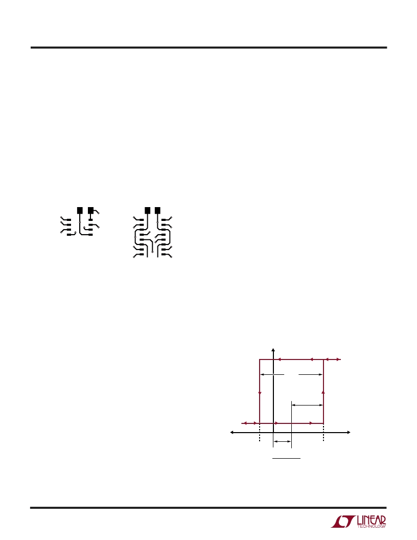
Figure 2. Hysteresis I/O Characteristics
The supply bypass should include an adjacent
10nF ceramic capacitor and a 2.2
μ
F tantalum capacitor no
farther than 5cm away; use more capacitance if driving
more than 4mA loads. To prevent oscillations, it is helpful
to balance the impedance at the inverting and noninverting
inputs; source impedances should be kept low, preferably
1k
or less.
The outputs of the LT1720/LT1721 are capable of very
high slew rates. To prevent overshoot, ringing and other
problems with transmission line effects, keep the output
traces shorter than 10cm, or be sure to terminate the lines
to maintain signal integrity. The LT1720/LT1721 can drive
DC terminations of 250
or more, but lower characteristic
impedance traces can be driven with series termination or
AC termination topologies.
Hysteresis
The LT1720/LT1721 include internal hysteresis, which
makes them easier to use than many other comparable
speed comparators.
The input-output transfer characteristic is illustrated in
Figure 2 showing the definitions of V
OS
and V
HYST
based
upon the two measurable trip points. The hysteresis band
makes the LT1720/LT1721 well behaved, even with slowly
moving inputs.
V
HYST
(= V
TRIP+
– V
TRIP–
)
V
HYST
/2
V
OL
1720/21 F02
V
OH
V
TRIP–
V
TRIP+
V
IN
= V
IN+
– V
IN–
V
TRIP+
+ V
TRIP–
2
V
OS
=
V
O
0
Figure 1. Typical Topside Metal for Multilayer PCB Layouts
1720/21 F01
(b)
(a)
Figure 1a shows a typical topside layout of the LT1720 on
such a multilayer board. Shown is the topside metal etch
including traces, pin escape vias, and the land pads for an
SO-8 LT1720 and its adjacent X7R 10nF bypass capacitor
in a 1206 case.
The ground trace from Pin 5 runs under the device up to
the bypass capacitor, shielding the inputs from the
outputs. Note the use of a common via for the LT1720 and
the bypass capacitor, which minimizes interference from
high frequency energy running around the ground plane or
power distribution traces.
Figure 1b shows a typical topside layout of the LT1721 on
a multilayer board. In this case, the power and ground
traces have been extended to the bottom of the device
solely to act as high frequency shields between input and
output traces.
Although both V
CC
pins are electrically shorted internal to
the LT1721, they must be shorted together externally as
well in order for both to function as shields. The same is
true for the two GND pins.
相关PDF资料 |
PDF描述 |
|---|---|
| LT1720CMS8 | Dual/Quad, 4.5ns, Single Supply 3V/5V Comparators with Rail-to-Rail Outputs |
| LT1721IS | Dual/Quad, 4.5ns, Single Supply 3V/5V Comparators with Rail-to-Rail Outputs |
| LT1722 | Single, Dual, Quad 200MHz Low Noise Precision Op Amps |
| LT1723CMS8 | Single, Dual, Quad 200MHz Low Noise Precision Op Amps |
| LT1723CS8 | Single, Dual, Quad 200MHz Low Noise Precision Op Amps |
相关代理商/技术参数 |
参数描述 |
|---|---|
| LT1720CS8#PBF | 功能描述:IC COMP R-RINOUT DUAL 8-SOIC RoHS:是 类别:集成电路 (IC) >> 线性 - 比较器 系列:UltraFast™ 标准包装:1 系列:- 类型:通用 元件数:1 输出类型:CMOS,开路集电极,TTL 电压 - 电源,单路/双路(±):2.7 V ~ 5.5 V 电压 - 输入偏移(最小值):7mV @ 5V 电流 - 输入偏压(最小值):0.25µA @ 5V 电流 - 输出(标准):84mA @ 5V 电流 - 静态(最大值):120µA CMRR, PSRR(标准):- 传输延迟(最大):600ns 磁滞:- 工作温度:-40°C ~ 85°C 封装/外壳:SC-74A,SOT-753 安装类型:表面贴装 包装:剪切带 (CT) 产品目录页面:1268 (CN2011-ZH PDF) 其它名称:*LMV331M5*LMV331M5/NOPBLMV331M5CT |
| LT1720CS8#PBF | 制造商:Linear Technology 功能描述:COMPARATOR DUAL R/R 3/5V 8SOIC 制造商:Linear Technology 功能描述:COMPARATOR, DUAL, R/R, 3/5V, 8SOIC |
| LT1720CS8#TR | 功能描述:IC COMP DUAL R-R 4MA 4.5NS 8SOIC RoHS:否 类别:集成电路 (IC) >> 线性 - 比较器 系列:UltraFast™ 产品培训模块:Lead (SnPb) Finish for COTS Obsolescence Mitigation Program 标准包装:2,500 系列:- 类型:通用 元件数:1 输出类型:CMOS,推挽式,满摆幅,TTL 电压 - 电源,单路/双路(±):2.5 V ~ 5.5 V,±1.25 V ~ 2.75 V 电压 - 输入偏移(最小值):5mV @ 5.5V 电流 - 输入偏压(最小值):1pA @ 5.5V 电流 - 输出(标准):- 电流 - 静态(最大值):24µA CMRR, PSRR(标准):80dB CMRR,80dB PSRR 传输延迟(最大):450ns 磁滞:±3mV 工作温度:-40°C ~ 85°C 封装/外壳:6-WFBGA,CSPBGA 安装类型:表面贴装 包装:管件 其它名称:Q3554586 |
| LT1720CS8#TRPBF | 功能描述:IC COMP R-RINOUT DUAL 8-SOIC RoHS:是 类别:集成电路 (IC) >> 线性 - 比较器 系列:UltraFast™ 产品培训模块:Lead (SnPb) Finish for COTS Obsolescence Mitigation Program 标准包装:2,500 系列:- 类型:通用 元件数:1 输出类型:CMOS,推挽式,满摆幅,TTL 电压 - 电源,单路/双路(±):2.5 V ~ 5.5 V,±1.25 V ~ 2.75 V 电压 - 输入偏移(最小值):5mV @ 5.5V 电流 - 输入偏压(最小值):1pA @ 5.5V 电流 - 输出(标准):- 电流 - 静态(最大值):24µA CMRR, PSRR(标准):80dB CMRR,80dB PSRR 传输延迟(最大):450ns 磁滞:±3mV 工作温度:-40°C ~ 85°C 封装/外壳:6-WFBGA,CSPBGA 安装类型:表面贴装 包装:管件 其它名称:Q3554586 |
| LT1720CS8PBF | 制造商:Linear Technology 功能描述:Comparator Dual 4.5ns RRO 3V/5V SOIC8 |
发布紧急采购,3分钟左右您将得到回复。