- 您现在的位置:买卖IC网 > PDF目录377712 > LT1721 (Linear Technology Corporation) Dual/Quad, 4.5ns, Single Supply 3V/5V Comparators with Rail-to-Rail Outputs PDF资料下载
参数资料
| 型号: | LT1721 |
| 厂商: | Linear Technology Corporation |
| 英文描述: | Dual/Quad, 4.5ns, Single Supply 3V/5V Comparators with Rail-to-Rail Outputs |
| 中文描述: | 双/四路,延迟时间为4.5ns,单电源3V/5V与铁比较到轨输出 |
| 文件页数: | 3/28页 |
| 文件大小: | 317K |
| 代理商: | LT1721 |
第1页第2页当前第3页第4页第5页第6页第7页第8页第9页第10页第11页第12页第13页第14页第15页第16页第17页第18页第19页第20页第21页第22页第23页第24页第25页第26页第27页第28页
3
LT1720/LT1721
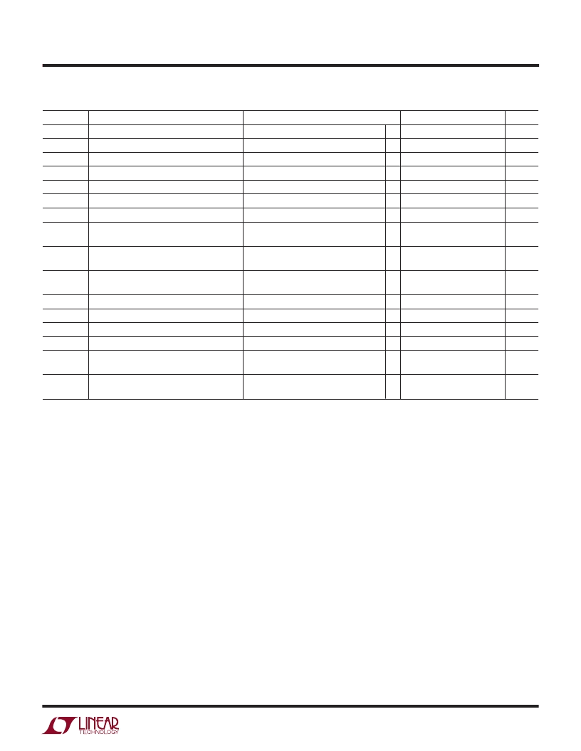
ELECTRICAL CHARACTERISTICS
range, otherwise specifications are at T
A
= 25
°
C. V
CC
= 5V, V
CM
= 1V, C
OUT
= 10pF, V
OVERDRIVE
= 20mV, unless otherwise specified.
The
G
denotes specifications that apply over the full operating temperature
SYMBOL
I
B
I
OS
CMRR
PSRR
A
V
V
OH
V
OL
I
CC
PARAMETER
Input Bias Current
Input Offset Current
Common Mode Rejection Ratio
Power Supply Rejection Ratio
Voltage Gain
Output High Voltage
Output Low Voltage
Supply Current (Per Comparator)
CONDITIONS
MIN
–6
TYP
MAX
0
0.6
UNITS
G
μ
A
μ
A
dB
dB
G
(Note 4)
(Note 5)
(Note 6)
I
SOURCE
= 4mA, V
IN
= V
TRIP+
+ 10mV
I
SINK
= 10mA, V
IN
= V
TRIP–
– 10mV
V
CC
= 5V
V
CC
= 3V
V
OVERDRIVE
= 20mV (Note 7)
G
55
65
70
80
∞
G
G
V
CC
– 0.4
V
V
G
0.4
7
6
6.5
8.0
10
13
1.0
1.5
G
G
4
mA
mA
ns
ns
ns
ns
ns
ns
ns
ns
3.5
4.5
t
PD20
Propagation Delay
G
t
PD5
Propagation Delay
V
OVERDRIVE
= 5mV (Notes 7, 8)
7
G
t
PD
t
SKEW
t
r
t
f
t
JITTER
Differential Propagation Delay
Propagation Delay Skew
Output Rise Time
Output Fall Time
Output Timing Jitter
(Note 9) Between Channels
(Note 10) Between t
PD+
/t
PD–
10% to 90%
90% to 10%
V
IN
= 1.2V
P-P
(6dBm), Z
IN
= 50
t
PD+
V
CM
= 2V, f = 20MHz t
PD–
V
OVERDRIVE
= 50mV, V
CC
= 3V
V
OVERDRIVE
= 50mV, V
CC
= 5V
0.3
0.5
2.5
2.2
15
11
70.0
62.5
ps
RMS
ps
RMS
MHz
MHz
f
MAX
Maximum Toggle Frequency
Note 1:
Absolute Maximum Ratings are those values beyond which the
life of a device may be impaired.
Note 2:
If one input is within these common mode limits, the other
input can go outside the common mode limits and the output will be
valid.
Note 3:
The LT1720/LT1721 comparators include internal hysteresis.
The trip points are the input voltage needed to change the output state
in each direction. The offset voltage is defined as the average of V
TRIP+
and V
TRIP–
, while the hysteresis voltage is the difference of these two.
Note 4:
The common mode rejection ratio is measured with V
CC
= 5V
and is defined as the change in offset voltage measured from V
CM
=
–0.1V to V
CM
= 3.8V, divided by 3.9V.
Note 5:
The power supply rejection ratio is measured with V
CM
= 1V
and is defined as the change in offset voltage measured from V
CC
=
2.7V to V
CC
= 6V, divided by 3.3V.
Note 6:
Because of internal hysteresis, there is no small-signal region
in which to measure gain. Proper operation of internal circuity is
ensured by measuring V
OH
and V
OL
with only 10mV of overdrive.
Note 7:
Propagation delay measurements made with 100mV steps.
Overdrive is measured relative to V
TRIP
±
.
Note 8:
t
PD
cannot be measured in automatic handling equipment with
low values of overdrive. The LT1720/LT1721 are 100% tested with a
100mV step and 20mV overdrive. Correlation tests have shown that
t
PD
limits can be guaranteed with this test, if additional DC tests are
performed to guarantee that all internal bias conditions are correct.
Note 9:
Differential propagation delay is defined as the larger of the
two:
t
PDLH
= t
PDLH(MAX)
– t
PDLH(MIN)
t
PDHL
= t
PDHL(MAX)
– t
PDHL(MIN)
where (MAX) and (MIN) denote the maximum and minimum values of
a given measurement across the different comparator channels.
Note 10:
Propagation Delay Skew is defined as:
t
SKEW
= |t
PDLH
– t
PDHL
|
相关PDF资料 |
PDF描述 |
|---|---|
| LT1721CGN | Dual/Quad, 4.5ns, Single Supply 3V/5V Comparators with Rail-to-Rail Outputs |
| LT1720CS8 | Dual/Quad, 4.5ns, Single Supply 3V/5V Comparators with Rail-to-Rail Outputs |
| LT1720CMS8 | Dual/Quad, 4.5ns, Single Supply 3V/5V Comparators with Rail-to-Rail Outputs |
| LT1721IS | Dual/Quad, 4.5ns, Single Supply 3V/5V Comparators with Rail-to-Rail Outputs |
| LT1722 | Single, Dual, Quad 200MHz Low Noise Precision Op Amps |
相关代理商/技术参数 |
参数描述 |
|---|---|
| LT1721CGN | 功能描述:IC COMP R-RINOUT QUAD 16-SSOP RoHS:否 类别:集成电路 (IC) >> 线性 - 比较器 系列:UltraFast™ 产品培训模块:Lead (SnPb) Finish for COTS Obsolescence Mitigation Program 标准包装:2,500 系列:- 类型:通用 元件数:1 输出类型:CMOS,推挽式,满摆幅,TTL 电压 - 电源,单路/双路(±):2.5 V ~ 5.5 V,±1.25 V ~ 2.75 V 电压 - 输入偏移(最小值):5mV @ 5.5V 电流 - 输入偏压(最小值):1pA @ 5.5V 电流 - 输出(标准):- 电流 - 静态(最大值):24µA CMRR, PSRR(标准):80dB CMRR,80dB PSRR 传输延迟(最大):450ns 磁滞:±3mV 工作温度:-40°C ~ 85°C 封装/外壳:6-WFBGA,CSPBGA 安装类型:表面贴装 包装:管件 其它名称:Q3554586 |
| LT1721CGN#PBF | 功能描述:IC COMP R-RINOUT QUAD 16-SSOP RoHS:是 类别:集成电路 (IC) >> 线性 - 比较器 系列:UltraFast™ 标准包装:1 系列:- 类型:通用 元件数:1 输出类型:CMOS,开路集电极,TTL 电压 - 电源,单路/双路(±):2.7 V ~ 5.5 V 电压 - 输入偏移(最小值):7mV @ 5V 电流 - 输入偏压(最小值):0.25µA @ 5V 电流 - 输出(标准):84mA @ 5V 电流 - 静态(最大值):120µA CMRR, PSRR(标准):- 传输延迟(最大):600ns 磁滞:- 工作温度:-40°C ~ 85°C 封装/外壳:SC-74A,SOT-753 安装类型:表面贴装 包装:剪切带 (CT) 产品目录页面:1268 (CN2011-ZH PDF) 其它名称:*LMV331M5*LMV331M5/NOPBLMV331M5CT |
| LT1721CGN#PBF | 制造商:Linear Technology 功能描述:High Speed Comparator IC |
| LT1721CGN#TR | 功能描述:IC COMP QUAD R-R 4.5NS 16SSOP RoHS:否 类别:集成电路 (IC) >> 线性 - 比较器 系列:UltraFast™ 产品培训模块:Lead (SnPb) Finish for COTS Obsolescence Mitigation Program 标准包装:2,500 系列:- 类型:通用 元件数:1 输出类型:CMOS,推挽式,满摆幅,TTL 电压 - 电源,单路/双路(±):2.5 V ~ 5.5 V,±1.25 V ~ 2.75 V 电压 - 输入偏移(最小值):5mV @ 5.5V 电流 - 输入偏压(最小值):1pA @ 5.5V 电流 - 输出(标准):- 电流 - 静态(最大值):24µA CMRR, PSRR(标准):80dB CMRR,80dB PSRR 传输延迟(最大):450ns 磁滞:±3mV 工作温度:-40°C ~ 85°C 封装/外壳:6-WFBGA,CSPBGA 安装类型:表面贴装 包装:管件 其它名称:Q3554586 |
| LT1721CGN#TRPBF | 功能描述:IC COMP R-RINOUT QUAD 16-SSOP RoHS:是 类别:集成电路 (IC) >> 线性 - 比较器 系列:UltraFast™ 产品培训模块:Lead (SnPb) Finish for COTS Obsolescence Mitigation Program 标准包装:2,500 系列:- 类型:通用 元件数:1 输出类型:CMOS,推挽式,满摆幅,TTL 电压 - 电源,单路/双路(±):2.5 V ~ 5.5 V,±1.25 V ~ 2.75 V 电压 - 输入偏移(最小值):5mV @ 5.5V 电流 - 输入偏压(最小值):1pA @ 5.5V 电流 - 输出(标准):- 电流 - 静态(最大值):24µA CMRR, PSRR(标准):80dB CMRR,80dB PSRR 传输延迟(最大):450ns 磁滞:±3mV 工作温度:-40°C ~ 85°C 封装/外壳:6-WFBGA,CSPBGA 安装类型:表面贴装 包装:管件 其它名称:Q3554586 |
发布紧急采购,3分钟左右您将得到回复。