- 您现在的位置:买卖IC网 > PDF目录377712 > LT1721CGN (LINEAR TECHNOLOGY CORP) Dual/Quad, 4.5ns, Single Supply 3V/5V Comparators with Rail-to-Rail Outputs PDF资料下载
参数资料
| 型号: | LT1721CGN |
| 厂商: | LINEAR TECHNOLOGY CORP |
| 元件分类: | 运动控制电子 |
| 英文描述: | Dual/Quad, 4.5ns, Single Supply 3V/5V Comparators with Rail-to-Rail Outputs |
| 中文描述: | QUAD COMPARATOR, 4500 uV OFFSET-MAX, 7 ns RESPONSE TIME, PDSO16 |
| 封装: | 0.150 INCH, PLASTIC, SSOP-16 |
| 文件页数: | 14/28页 |
| 文件大小: | 317K |
| 代理商: | LT1721CGN |
第1页第2页第3页第4页第5页第6页第7页第8页第9页第10页第11页第12页第13页当前第14页第15页第16页第17页第18页第19页第20页第21页第22页第23页第24页第25页第26页第27页第28页
14
LT1720/LT1721
–
+
–
+
–
+
C1
1/2 LT1720
C2
1/2 LT1720
LTA1
V
2.7V TO 6V
2k
620
220
1MHz TO 10MHz
CRYSTAL (AT-CUT)
100k
100k
1720 F07
1.8k
2k
1k
0.1
μ
F
0.1
μ
F
0.1
μ
F
OUTPUT
OUTPUT
GROUND
CASE
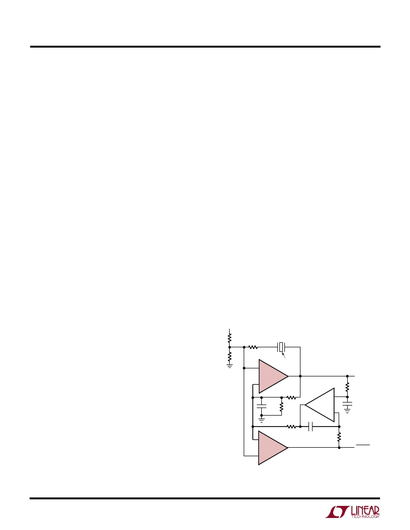
Figure 7. Crystal Oscillator with Complementary
Outputs and 50% Duty Cycle
APPLICATIO
S I
N
FOR
ATIO
U
fast enough that the absolute dispersion of 2.5ns
(= 7 – 4.5) is often small enough to ignore.
The gain and hysteresis stage of the LT1720/LT1721 is
simple, short and high speed to help prevent parasitic
oscillations while adding minimum dispersion. This in-
ternal “self-latch” can be usefully exploited in many
applications because it occurs early in the signal chain, in
a low power, fully differential stage. It is therefore highly
immune to disturbances from other parts of the circuit,
either in the same comparator, on the supply lines, or
from the other comparator(s) in the same package. Once
a high speed signal trips the hysteresis, the output will
respond, after a fixed propagation delay, without regard
to these external influences that can cause trouble in
nonhysteretic comparators.
W
U
±
V
TRIP
Test Circuit
The input trip points are tested using the circuit shown in
the Test Circuits section that precedes this Applications
Information section. The test circuit uses a 1kHz triangle
wave to repeatedly trip the comparator being tested. The
LT1720/LT1721 output is used to trigger switched capaci-
tor sampling of the triangle wave, with a sampler for each
direction. Because the triangle wave is attenuated 1000:1
and fed to the LT1720/LT1721’s differential input, the
sampled voltages are therefore 1000 times the input trip
voltages. The hysteresis and offset are computed from the
trip points as shown.
Crystal Oscillators
A simple crystal oscillator using one comparator of an
LT1720/LT1721 is shown on the first page of this data
sheet. The 2k-620
resistor pair set a bias point at the
comparator’s noninverting input. The 2k-1.8k-0.1
μ
F path
sets the inverting input node at an appropriate DC average
level based on the output. The crystal’s path provides
resonant positive feedback and stable oscillation occurs.
Although the LT1720/LT1721 will give the correct logic
output when one input is outside the common mode
range, additional delays may occur when it is so operated,
opening the possibility of spurious operating modes.
Therefore, the DC bias voltages at the inputs are set near
the center of the LT1720/LT1721’s common mode range
and the 220
resistor attenuates the feedback to the
noninverting input. The circuit will operate with any AT-cut
crystal from 1MHz to 10MHz over a 2.7V to 6V supply
range. As the power is applied, the circuit remains off until
the LT1720/LT1721 bias circuits activate, at a typical V
CC
of 2V to 2.2V (25
°
C), at which point the desired frequency
output is generated.
The output duty cycle for this circuit is roughly 50%, but
it is affected by resistor tolerances and, to a lesser extent,
by comparator offsets and timings. If a 50% duty cycle is
required, the circuit of Figure 7 creates a pair of comple-
mentary outputs with a forced 50% duty cycle. Crystals
are narrow-band elements, so the feedback to the nonin-
verting input is a filtered analog version of the square wave
output. Changing the noninverting reference level can there-
fore vary the duty cycle. C1 operates as in the previous
example, whereas C2 creates a complementary output by
comparing the same two nodes with the opposite input
polarity. A1 compares band-limited versions of the out-
puts and biases C1’s negative input. C1’s only degree of
freedom to respond is variation of pulse width; hence the
outputs are forced to 50% duty cycle. Again, the circuit
operates from 2.7V to 6V, and the skew between the edges
of the two outputs are shown in Figure 8. There is a slight
duty cycle dependence on comparator loading, so equal
capacitive and resistive loading should be used in critical
相关PDF资料 |
PDF描述 |
|---|---|
| LT1720CS8 | Dual/Quad, 4.5ns, Single Supply 3V/5V Comparators with Rail-to-Rail Outputs |
| LT1720CMS8 | Dual/Quad, 4.5ns, Single Supply 3V/5V Comparators with Rail-to-Rail Outputs |
| LT1721IS | Dual/Quad, 4.5ns, Single Supply 3V/5V Comparators with Rail-to-Rail Outputs |
| LT1722 | Single, Dual, Quad 200MHz Low Noise Precision Op Amps |
| LT1723CMS8 | Single, Dual, Quad 200MHz Low Noise Precision Op Amps |
相关代理商/技术参数 |
参数描述 |
|---|---|
| LT1721CGN#PBF | 功能描述:IC COMP R-RINOUT QUAD 16-SSOP RoHS:是 类别:集成电路 (IC) >> 线性 - 比较器 系列:UltraFast™ 标准包装:1 系列:- 类型:通用 元件数:1 输出类型:CMOS,开路集电极,TTL 电压 - 电源,单路/双路(±):2.7 V ~ 5.5 V 电压 - 输入偏移(最小值):7mV @ 5V 电流 - 输入偏压(最小值):0.25µA @ 5V 电流 - 输出(标准):84mA @ 5V 电流 - 静态(最大值):120µA CMRR, PSRR(标准):- 传输延迟(最大):600ns 磁滞:- 工作温度:-40°C ~ 85°C 封装/外壳:SC-74A,SOT-753 安装类型:表面贴装 包装:剪切带 (CT) 产品目录页面:1268 (CN2011-ZH PDF) 其它名称:*LMV331M5*LMV331M5/NOPBLMV331M5CT |
| LT1721CGN#PBF | 制造商:Linear Technology 功能描述:High Speed Comparator IC |
| LT1721CGN#TR | 功能描述:IC COMP QUAD R-R 4.5NS 16SSOP RoHS:否 类别:集成电路 (IC) >> 线性 - 比较器 系列:UltraFast™ 产品培训模块:Lead (SnPb) Finish for COTS Obsolescence Mitigation Program 标准包装:2,500 系列:- 类型:通用 元件数:1 输出类型:CMOS,推挽式,满摆幅,TTL 电压 - 电源,单路/双路(±):2.5 V ~ 5.5 V,±1.25 V ~ 2.75 V 电压 - 输入偏移(最小值):5mV @ 5.5V 电流 - 输入偏压(最小值):1pA @ 5.5V 电流 - 输出(标准):- 电流 - 静态(最大值):24µA CMRR, PSRR(标准):80dB CMRR,80dB PSRR 传输延迟(最大):450ns 磁滞:±3mV 工作温度:-40°C ~ 85°C 封装/外壳:6-WFBGA,CSPBGA 安装类型:表面贴装 包装:管件 其它名称:Q3554586 |
| LT1721CGN#TRPBF | 功能描述:IC COMP R-RINOUT QUAD 16-SSOP RoHS:是 类别:集成电路 (IC) >> 线性 - 比较器 系列:UltraFast™ 产品培训模块:Lead (SnPb) Finish for COTS Obsolescence Mitigation Program 标准包装:2,500 系列:- 类型:通用 元件数:1 输出类型:CMOS,推挽式,满摆幅,TTL 电压 - 电源,单路/双路(±):2.5 V ~ 5.5 V,±1.25 V ~ 2.75 V 电压 - 输入偏移(最小值):5mV @ 5.5V 电流 - 输入偏压(最小值):1pA @ 5.5V 电流 - 输出(标准):- 电流 - 静态(最大值):24µA CMRR, PSRR(标准):80dB CMRR,80dB PSRR 传输延迟(最大):450ns 磁滞:±3mV 工作温度:-40°C ~ 85°C 封装/外壳:6-WFBGA,CSPBGA 安装类型:表面贴装 包装:管件 其它名称:Q3554586 |
| LT1721CS | 功能描述:IC COMP R-RINOUT QUAD 16-SOIC RoHS:否 类别:集成电路 (IC) >> 线性 - 比较器 系列:UltraFast™ 产品培训模块:Lead (SnPb) Finish for COTS Obsolescence Mitigation Program 标准包装:2,500 系列:- 类型:通用 元件数:1 输出类型:CMOS,推挽式,满摆幅,TTL 电压 - 电源,单路/双路(±):2.5 V ~ 5.5 V,±1.25 V ~ 2.75 V 电压 - 输入偏移(最小值):5mV @ 5.5V 电流 - 输入偏压(最小值):1pA @ 5.5V 电流 - 输出(标准):- 电流 - 静态(最大值):24µA CMRR, PSRR(标准):80dB CMRR,80dB PSRR 传输延迟(最大):450ns 磁滞:±3mV 工作温度:-40°C ~ 85°C 封装/外壳:6-WFBGA,CSPBGA 安装类型:表面贴装 包装:管件 其它名称:Q3554586 |
发布紧急采购,3分钟左右您将得到回复。