- 您现在的位置:买卖IC网 > PDF目录10679 > LT1721IS (Linear Technology)IC COMP R-RINOUT QUAD 16-SOIC PDF资料下载
参数资料
| 型号: | LT1721IS |
| 厂商: | Linear Technology |
| 文件页数: | 5/28页 |
| 文件大小: | 0K |
| 描述: | IC COMP R-RINOUT QUAD 16-SOIC |
| 标准包装: | 50 |
| 系列: | UltraFast™ |
| 类型: | 通用 |
| 元件数: | 4 |
| 输出类型: | CMOS,满摆幅,TTL |
| 电压 - 电源,单路/双路(±): | 2.7 V ~ 6 V |
| 电压 - 输入偏移(最小值): | 3mV @ 5V |
| 电流 - 输入偏压(最小值): | 6µA @ 5V |
| 电流 - 输出(标准): | 20mA |
| 电流 - 静态(最大值): | 7mA |
| CMRR, PSRR(标准): | 70dB CMRR,80dB PSRR |
| 传输延迟(最大): | 10ns |
| 磁滞: | 7mV |
| 工作温度: | -40°C ~ 85°C |
| 封装/外壳: | 16-SOIC(0.154",3.90mm 宽) |
| 安装类型: | 表面贴装 |
| 包装: | 管件 |
第1页第2页第3页第4页当前第5页第6页第7页第8页第9页第10页第11页第12页第13页第14页第15页第16页第17页第18页第19页第20页第21页第22页第23页第24页第25页第26页第27页第28页
LT1720/LT1721
13
17201fc
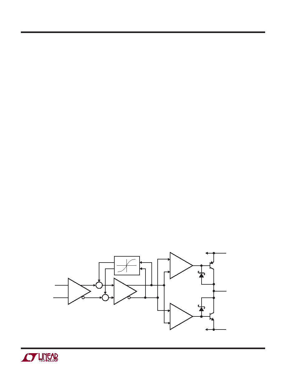
Circuit Description
The block diagram of one comparator in the LT1720/LT1721
is shown in Figure 6. There are differential inputs (+IN/–IN),
an output (OUT), a single positive supply (VCC) and ground
(GND). All comparators are completely independent, shar-
ing only the power and ground pins. The circuit topology
consists of a differential input stage, a gain stage with
hysteresis and a complementary common-emitter output
stage. All of the internal signal paths utilize low voltage
swings for high speed at low power.
The input stage topology maximizes the input dynamic
range available without requiring the power, complex-
ity and die area of two complete input stages such as
are found in rail-to-rail input comparators. With a 2.7V
supply, the LT1720/LT1721 still have a respectable 1.6V
of input common mode range. The differential input volt-
age range is rail-to-rail, without the large input currents
found in competing devices. The input stage also features
phase reversal protection to prevent false outputs when
the inputs are driven below the –100mV common mode
voltage limit.
The internal hysteresis is implemented by positive, nonlin-
ear feedback around a second gain stage. Until this point,
the signal path has been entirely differential. The signal
path is then split into two drive signals for the upper and
lower output transistors. The output transistors are con-
nected common emitter for rail-to-rail output operation.
The Schottky clamps limit the output voltages at about
300mV from the rail, not quite the 50mV or 15mV of Linear
APPLICATIONS INFORMATION
Technology’s rail-to-rail ampliers and other products. But
the output of a comparator is digital, and this output stage
can drive TTL or CMOS directly. It can also drive ECL, as
described earlier, or analog loads as demonstrated in the
applications to follow.
The bias conditions and signal swings in the output stages
are designed to turn their respective output transistors off
faster than on. This nearly eliminates the surge of current
from VCC to ground that occurs at transitions, keeping
the power consumption low even with high output-toggle
frequencies.
The low surge current is what keeps the power consump-
tion low at high output-toggle frequencies. The frequency
dependence of the supply current is shown in the Typical
Performance Characteristics. Just 20pF of capacitive load
on the output more than triples the frequency dependent
rise. The slope of the no-load curve is just 32μA/MHz. With
a 5V supply, this current is the equivalent of charging and
discharging just 6.5pF. The slope of the 20pF load curve is
133μA/MHz, an addition of 101μA/MHz, or 20μA/MHz-V,
units that are equivalent to picoFarads.
The LT1720/LT1721 dynamic current can be estimated
by adding the external capacitive loading to an internal
equivalent capacitance of 5pF to 15pF, multiplied by the
toggle frequency and the supply voltage. Because the
capacitance of routing traces can easily approach these
values, the dynamic current is dominated by the load in
most circuits.
Figure 6. LT1720/LT1721 Block Diagram
–
+
–
+
–
+
–
+
+IN
–IN
AV1
AV2
NONLINEAR STAGE
OUT
GND
17201 F06
VCC
+
相关PDF资料 |
PDF描述 |
|---|---|
| LT1721CGN#TRPBF | IC COMP R-RINOUT QUAD 16-SSOP |
| 85100JC1210PZ50 | CONN RCPT WALL MT 10POS W/PIN |
| LT1016IN8#PBF | IC COMPARATOR 10NS HI-SPEED 8DIP |
| VI-J2Y-MY-F3 | CONVERTER MOD DC/DC 3.3V 33W |
| VI-J2Y-MY-F4 | CONVERTER MOD DC/DC 3.3V 33W |
相关代理商/技术参数 |
参数描述 |
|---|---|
| LT1721IS#PBF | 功能描述:IC COMP R-RINOUT QUAD 16-SOIC RoHS:是 类别:集成电路 (IC) >> 线性 - 比较器 系列:UltraFast™ 产品培训模块:Lead (SnPb) Finish for COTS Obsolescence Mitigation Program 标准包装:2,500 系列:- 类型:通用 元件数:1 输出类型:CMOS,推挽式,满摆幅,TTL 电压 - 电源,单路/双路(±):2.5 V ~ 5.5 V,±1.25 V ~ 2.75 V 电压 - 输入偏移(最小值):5mV @ 5.5V 电流 - 输入偏压(最小值):1pA @ 5.5V 电流 - 输出(标准):- 电流 - 静态(最大值):24µA CMRR, PSRR(标准):80dB CMRR,80dB PSRR 传输延迟(最大):450ns 磁滞:±3mV 工作温度:-40°C ~ 85°C 封装/外壳:6-WFBGA,CSPBGA 安装类型:表面贴装 包装:管件 其它名称:Q3554586 |
| LT1721IS#TRPBF | 制造商:Linear Technology 功能描述:Comparator Quad R-R O/P 6V 16-Pin SOIC N T/R 制造商:Linear Technology 功能描述:IC COMP R-RINOUT QUAD 16SOIC |
| LT1722 | 制造商:LINER 制造商全称:Linear Technology 功能描述:Single, Dual, Quad 200MHz Low Noise Precision Op Amps |
| LT1722CS5 | 制造商:Linear Technology 功能描述:OP Amp Single GP ±6.3V/12.6V 5-Pin TSOT-23 |
| LT1722CS5#PBF | 制造商:Linear Technology 功能描述:OP Amp Single GP 制造商:Linear Technology 功能描述:SC-Amps/Industrial Cut Tape 2 制造商:Linear Technology 功能描述:SC-Amps/Industrial, Cut Tape 200MHz Low Noise Precision OP Amp |
发布紧急采购,3分钟左右您将得到回复。