- 您现在的位置:买卖IC网 > PDF目录377712 > LT1723CS8 (LINEAR TECHNOLOGY CORP) Single, Dual, Quad 200MHz Low Noise Precision Op Amps PDF资料下载
参数资料
| 型号: | LT1723CS8 |
| 厂商: | LINEAR TECHNOLOGY CORP |
| 元件分类: | 运动控制电子 |
| 英文描述: | Single, Dual, Quad 200MHz Low Noise Precision Op Amps |
| 中文描述: | DUAL OP-AMP, 700 uV OFFSET-MAX, 200 MHz BAND WIDTH, PDSO8 |
| 封装: | 0.150 INCH, PLASTIC, SO-8 |
| 文件页数: | 12/16页 |
| 文件大小: | 326K |
| 代理商: | LT1723CS8 |
LT1722/LT1723/LT1724
12
172234fa
APPLICATIU
W
U
U
The LT1722/LT1723/LT1724 may be inserted directly into
many operational amplifier applications improving both
DC and AC performance, as well as noise and distortion.
Layout and Passive Components
The LT1722/LT1723/LT1724 amplifiers are more tolerant
of less than ideal layouts than other high speed amplifiers.
For maximum performance (for example, fast settling
time) use a ground plane, short lead lengths and RF quality
bypass capacitors (0.01
μ
F to 0.1
μ
F). For high drive cur-
rent applications, use low ESR supply bypass capacitors
(1
μ
F to 10
μ
F tantalum). The output/input parasitic cou-
pling should be minimized when high frequency perfor-
mance is required.
The parallel combination of the feedback resistor and gain
setting resistor on the inverting input combine with the
input capacitance to form a pole that can cause peaking or
even oscillations. In parallel with the feedback resistor, a
capacitor of value:
C
F
> R
G
C
IN
/R
F
should be used to cancel the input pole and optimize
dynamic performance. For unity-gain applications where
a feedback resistor is used, such as an I-to-V converter, C
F
should be five times greater than C
IN
; an optimum value for
C
F
is 10pF.
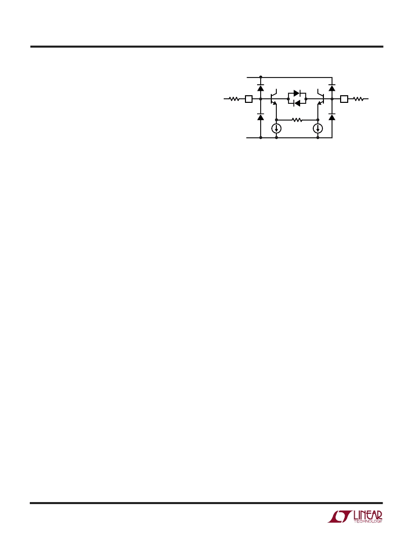
Input Considerations
Each of the LT1722/LT1723/LT1724 inputs is protected
with back-to-back diodes across the bases of the NPN
input devices. If greater than 0.7V differential input volt-
ages are anticipated, the input current must be limited to
less than 10mA with an external series resistor. Each input
also has two ESD clamp diodes—one to each supply. If an
input is driven beyond the supply, limit the current with an
external resistor to less than 10mA. The input stage
protection circuit is shown in Figure 1.
The input currents of the LT1722/LT1723/LT1724 are
typically in the tens of nA range due to the bias current
cancellation technique used at the input. As the input
offset current can be greater than either input current,
D1
D3
+IN
+IN
D4
D5
D6
1723 F01
D2
R
I
1
I
2
Q1
R
EXT
Q2
V
S+
V
S–
–IN
–IN
R
EXT
Figure 1. Input Stage Protection
adding resistance to balance source resistance is not
recommended. The value of the source resistor should be
below 12k as it actually degrades DC accuracy and also
increases noise.
Total Input Noise
The total input noise of the LT1722/LT1723/LT1724 is
optimized for a source resistance between 0.8k and 12k.
Within this range, the total input noise is dominated by the
noise of the source resistance itself. When the source
resistance is below 0.8k, voltage noise of the amplifier
dominates. When the source resistance is above 12k, the
input noise current is the dominant contributor.
Capacitive Loading
The
LT1722/LT1723/LT1724
drive capacitive loads up to
100pF with unity gain. As the capacitive load increases,
both the bandwidth and the phase margin decrease
causing peaking in the frequency response and overshoot
in the transient response. When there is a need to drive a
larger capacitive load, a 25
series resistance assures
stability with any value of load capacitor. A feedback
capacitor also helps to reduce any peaking.
Power Dissipation
The LT1722/LT1723/LT1724 combine high speed and
large output drive in a small package. Maximum junction
temperature (T
J
) is calculated from the ambient tempera-
ture (T
A
), power dissipation per amplifier (P
D
) and number
of amplifiers (n) as follows:
T
J
= T
A
+ (n P
D
θ
JA
)
相关PDF资料 |
PDF描述 |
|---|---|
| LT1723IMS8 | Single, Dual, Quad 200MHz Low Noise Precision Op Amps |
| LT1723IS8 | Single, Dual, Quad 200MHz Low Noise Precision Op Amps |
| LT1724CS | Single, Dual, Quad 200MHz Low Noise Precision Op Amps |
| LT1724IS | Single, Dual, Quad 200MHz Low Noise Precision Op Amps |
| LT1722CS5 | Single, Dual, Quad 200MHz Low Noise Precision Op Amps |
相关代理商/技术参数 |
参数描述 |
|---|---|
| LT1723CS8#PBF | 功能描述:IC PREC OPAMP 200MHZ DUAL 8-SOIC RoHS:是 类别:集成电路 (IC) >> Linear - Amplifiers - Instrumentation 系列:- 标准包装:2,500 系列:- 放大器类型:通用 电路数:1 输出类型:满摆幅 转换速率:0.11 V/µs 增益带宽积:350kHz -3db带宽:- 电流 - 输入偏压:4nA 电压 - 输入偏移:20µV 电流 - 电源:260µA 电流 - 输出 / 通道:20mA 电压 - 电源,单路/双路(±):2.7 V ~ 36 V,±1.35 V ~ 18 V 工作温度:-40°C ~ 85°C 安装类型:表面贴装 封装/外壳:8-SOIC(0.154",3.90mm 宽) 供应商设备封装:8-SO 包装:带卷 (TR) |
| LT1723CS8#TR | 功能描述:IC PREC OPAMP 200MHZ DUAL 8-SOIC RoHS:否 类别:集成电路 (IC) >> Linear - Amplifiers - Instrumentation 系列:- 标准包装:2,500 系列:- 放大器类型:通用 电路数:1 输出类型:满摆幅 转换速率:0.11 V/µs 增益带宽积:350kHz -3db带宽:- 电流 - 输入偏压:4nA 电压 - 输入偏移:20µV 电流 - 电源:260µA 电流 - 输出 / 通道:20mA 电压 - 电源,单路/双路(±):2.7 V ~ 36 V,±1.35 V ~ 18 V 工作温度:-40°C ~ 85°C 安装类型:表面贴装 封装/外壳:8-SOIC(0.154",3.90mm 宽) 供应商设备封装:8-SO 包装:带卷 (TR) |
| LT1723CS8#TRPBF | 功能描述:IC PREC OPAMP 200MHZ DUAL 8-SOIC RoHS:是 类别:集成电路 (IC) >> Linear - Amplifiers - Instrumentation 系列:- 标准包装:2,500 系列:- 放大器类型:通用 电路数:1 输出类型:满摆幅 转换速率:0.11 V/µs 增益带宽积:350kHz -3db带宽:- 电流 - 输入偏压:4nA 电压 - 输入偏移:20µV 电流 - 电源:260µA 电流 - 输出 / 通道:20mA 电压 - 电源,单路/双路(±):2.7 V ~ 36 V,±1.35 V ~ 18 V 工作温度:-40°C ~ 85°C 安装类型:表面贴装 封装/外壳:8-SOIC(0.154",3.90mm 宽) 供应商设备封装:8-SO 包装:带卷 (TR) |
| LT1723IMS8 | 功能描述:IC OPAMP PREC DUAL 200MHZ 8MSOP RoHS:否 类别:集成电路 (IC) >> Linear - Amplifiers - Instrumentation 系列:- 标准包装:1,000 系列:- 放大器类型:电压反馈 电路数:4 输出类型:满摆幅 转换速率:33 V/µs 增益带宽积:20MHz -3db带宽:30MHz 电流 - 输入偏压:2nA 电压 - 输入偏移:3000µV 电流 - 电源:2.5mA 电流 - 输出 / 通道:30mA 电压 - 电源,单路/双路(±):4.5 V ~ 16.5 V,±2.25 V ~ 8.25 V 工作温度:-40°C ~ 85°C 安装类型:表面贴装 封装/外壳:14-SOIC(0.154",3.90mm 宽) 供应商设备封装:14-SOIC 包装:带卷 (TR) |
| LT1723IMS8#PBF | 功能描述:IC OPAMP PREC DUAL 200MHZ 8MSOP RoHS:是 类别:集成电路 (IC) >> Linear - Amplifiers - Instrumentation 系列:- 标准包装:1,000 系列:- 放大器类型:电压反馈 电路数:4 输出类型:满摆幅 转换速率:33 V/µs 增益带宽积:20MHz -3db带宽:30MHz 电流 - 输入偏压:2nA 电压 - 输入偏移:3000µV 电流 - 电源:2.5mA 电流 - 输出 / 通道:30mA 电压 - 电源,单路/双路(±):4.5 V ~ 16.5 V,±2.25 V ~ 8.25 V 工作温度:-40°C ~ 85°C 安装类型:表面贴装 封装/外壳:14-SOIC(0.154",3.90mm 宽) 供应商设备封装:14-SOIC 包装:带卷 (TR) |
发布紧急采购,3分钟左右您将得到回复。