- 您现在的位置:买卖IC网 > PDF目录10066 > LT1739CFE#TRPBF (Linear Technology)IC AMP XDSL LINE DRV DUAL20TSSOP PDF资料下载
参数资料
| 型号: | LT1739CFE#TRPBF |
| 厂商: | Linear Technology |
| 文件页数: | 4/20页 |
| 文件大小: | 0K |
| 描述: | IC AMP XDSL LINE DRV DUAL20TSSOP |
| 标准包装: | 2,500 |
| 类型: | 线路驱动器,发射器 |
| 驱动器/接收器数: | 2/0 |
| 规程: | DSL |
| 电源电压: | 5 V ~ 12 V |
| 安装类型: | 表面贴装 |
| 封装/外壳: | 20-TSSOP(0.173",4.40mm 宽)裸露焊盘 |
| 供应商设备封装: | 20-TSSOP-EP |
| 包装: | 带卷 (TR) |
12
LT1739
1739fas, sn1739
Layout and Passive Components
With a gain bandwidth product of 200MHz the LT1739
requires attention to detail in order to extract maximum
performance. Use a ground plane, short lead lengths and
a combination of RF-quality supply bypass capacitors (i.e.,
0.1
F). As the primary applications have high drive cur-
rent, use low ESR supply bypass capacitors (1
F to 10F).
The parallel combination of the feedback resistor and gain
setting resistor on the inverting input can combine with the
input capacitance to form a pole that can cause frequency
peaking. In general, use feedback resistors of 1k or less.
Compensation
The LT1739 is stable in a gain 10 or higher for any supply
and resistive load. It is easily compensated for lower gains
with a single resistor or a resistor plus a capacitor.
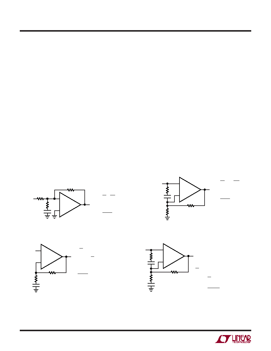
Figure 9 shows that for inverting gains, a resistor from the
inverting node to AC ground guarantees stability if the
parallel combination of RC and RG is less than or equal to
RF/9. For lowest distortion and DC output offset, a series
capacitor, CC, can be used to reduce the noise gain at
lower frequencies. The break frequency produced by RC
and CC should be less than 5MHz to minimize peaking.
Figure 10 shows compensation in the noninverting con-
figuration. The RC, CC network acts similarly to the invert-
ing case. The input impedance is not reduced because the
network is bootstrapped. This network can also be placed
between the inverting input and an AC ground.
Another compensation scheme for noninverting circuits is
shown in Figure 11. The circuit is unity gain at low
frequency and a gain of 1 + RF/RG at high frequency. The
DC output offset is reduced by a factor of ten. The
techniques of Figures 10 and 11 can be combined as
shown in Figure 12. The gain is unity at low frequencies,
1 + RF/RG at mid-band and for stability, a gain of 10 or
greater at high frequencies.
Figure 9. Compensation for Inverting Gains
APPLICATIO S I FOR ATIO
WU
UU
RG
RC
VO
VI
CC
(OPTIONAL)
–
+
1739 F09
RF
=
–RF
RG
VO
VI
< 5MHz
1
2
πRCCC
(RC || RG) ≤ RF/9
RC
VO
VI
CC
(OPTIONAL)
+
–
1739 F10
RF
RG
= 1 +
RF
RG
VO
VI
< 5MHz
1
2
πRCCC
(RC || RG) ≤ RF/9
Figure 10. Compensation for Noninverting Gains
+
–
1739 F11
RF
RG
Vi
VO
CC
< 5MHz
1
2
πRGCC
RG ≤ RF/9
= 1 (LOW FREQUENCIES)
(HIGH FREQUENCIES)
VO
VI
= 1 +
RF
RG
Figure 11. Alternate Noninverting Compensation
RC
VO
VI
CC
+
–
1739 F12
RF
RG
CBIG
RF
RG
= 1 AT LOW FREQUENCIES
= 1 +
AT MEDIUM FREQUENCIES
RF
(RC || RG)
= 1 +
AT HIGH FREQUENCIES
VO
VI
Figure 12. Combination Compensation
相关PDF资料 |
PDF描述 |
|---|---|
| LT1739CFE#TR | IC AMP XDSL LINE DRV DUAL20TSSOP |
| MS27497T12F35P | CONN RCPT 22POS WALL MNT W/PINS |
| IDT72V231L15PFGI | IC FIFO SYNC 2048X9 15NS 32-TQFP |
| LTC1385ISW#PBF | IC TXRX 3.3V EIA/TIA-562 18-SOIC |
| MS27499E10B35SA | CONN RCPT 13POS BOX MNT W/SCKT |
相关代理商/技术参数 |
参数描述 |
|---|---|
| LT1739CUE | 制造商:LINER 制造商全称:Linear Technology 功能描述:Dual 500mA, 200MHz xDSL Line Driver Amplifier |
| LT1739CUE#PBF | 功能描述:IC OP AMP XDSL DVR 500MA 12DFN RoHS:是 类别:集成电路 (IC) >> 接口 - 驱动器,接收器,收发器 系列:* 标准包装:27 系列:- 类型:收发器 驱动器/接收器数:3/3 规程:RS232,RS485 电源电压:4.75 V ~ 5.25 V 安装类型:表面贴装 封装/外壳:28-SOIC(0.295",7.50mm 宽) 供应商设备封装:28-SOIC 包装:管件 |
| LT1739CUE#TR | 功能描述:IC AMP XDSL LINE DVR DUAL 12-DFN RoHS:否 类别:集成电路 (IC) >> 接口 - 驱动器,接收器,收发器 系列:- 标准包装:27 系列:- 类型:收发器 驱动器/接收器数:3/3 规程:RS232,RS485 电源电压:4.75 V ~ 5.25 V 安装类型:表面贴装 封装/外壳:28-SOIC(0.295",7.50mm 宽) 供应商设备封装:28-SOIC 包装:管件 |
| LT1739CUE#TRPBF | 功能描述:IC AMP XDSL LINE DVR DUAL 12-DFN RoHS:是 类别:集成电路 (IC) >> 接口 - 驱动器,接收器,收发器 系列:- 标准包装:27 系列:- 类型:收发器 驱动器/接收器数:3/3 规程:RS232,RS485 电源电压:4.75 V ~ 5.25 V 安装类型:表面贴装 封装/外壳:28-SOIC(0.295",7.50mm 宽) 供应商设备封装:28-SOIC 包装:管件 |
| LT1739IFE | 功能描述:IC AMP XDSL LINE DRV DUAL20TSSOP RoHS:否 类别:集成电路 (IC) >> 接口 - 驱动器,接收器,收发器 系列:- 标准包装:27 系列:- 类型:收发器 驱动器/接收器数:3/3 规程:RS232,RS485 电源电压:4.75 V ~ 5.25 V 安装类型:表面贴装 封装/外壳:28-SOIC(0.295",7.50mm 宽) 供应商设备封装:28-SOIC 包装:管件 |
发布紧急采购,3分钟左右您将得到回复。