参数资料
| 型号: | LT1763IDE-1.5#PBF |
| 厂商: | Linear Technology |
| 文件页数: | 14/22页 |
| 文件大小: | 0K |
| 描述: | IC REG LDO 1.5V .5A 12DFN |
| 标准包装: | 91 |
| 稳压器拓扑结构: | 正,固定式 |
| 输出电压: | 1.5V |
| 输入电压: | 1.8 V ~ 20 V |
| 电压 - 压降(标准): | 0.3V @ 500mA |
| 稳压器数量: | 1 |
| 电流 - 输出: | 500mA |
| 电流 - 限制(最小): | 520mA |
| 工作温度: | -40°C ~ 125°C |
| 安装类型: | 表面贴装 |
| 封装/外壳: | 12-WFDFN 裸露焊盘 |
| 供应商设备封装: | 12-DFN(4x3) |
| 包装: | 管件 |
�� ��
��
��LT1763� Series�
�PIN� FUNCTIONS�
�(DE12/S8)�
�NC� (Pins� 1,� 4,� 9,� 12)� DE12� Only:� No� Connect.� No� connect�
�pins� have� no� connection� to� any� internal� circuitry.� These�
�pins� may� be� tied� to� either� GND� or� V� IN� ,� or� left� ?oating.�
�OUT� (Pins� 2,� 3/Pin� 1):� Output.� The� output� supplies� power�
�to� the� load.� A� minimum� output� capacitor� of� 3.3μF� is� re-�
�quired� to� prevent� oscillations.� Larger� output� capacitors�
�will� be� required� for� applications� with� large� transient� loads�
�to� limit� peak� voltage� transients.� See� the� Applications� Infor-�
�mation� section� for� more� information� on� output� capacitance�
�and� reverse� output� characteristics.�
�ADJ� (Pin� 5/Pin� 2):� Adjust.� For� the� adjustable� LT1763,� this�
�is� the� input� to� the� error� ampli?er.� This� pin� is� internally�
�clamped� to� ±7V.� It� has� a� bias� current� of� 30nA� which� ?ows�
�into� the� pin� (see� the� curve� of� ADJ� Pin� Bias� Current� vs�
�Temperature� in� the� Typical� Performance� Characteristics�
�section).� The� ADJ� pin� voltage� is� 1.22V� referenced� to� ground�
�and� the� output� voltage� range� is� 1.22V� to� 20V.�
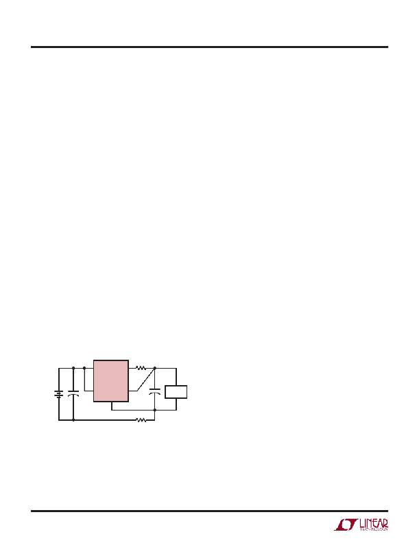
�SENSE� (Pin� 5/Pin� 2):� Output� Sense.� For� ?xed� volt-�
�age� versions� of� the� LT1763� (LT1763-1.5/LT1763-1.8/�
�LT1763-2.5/LT1763-3/LT1763-3.3/LT1763-5),� the� SENSE�
�pin� is� the� input� to� the� error� ampli?er.� Optimum� regula-�
�tion� will� be� obtained� at� the� point� where� the� SENSE� pin�
�is� connected� to� the� OUT� pin� of� the� regulator.� In� critical�
�applications,� small� voltage� drops� are� caused� by� the� re-�
�sistance� (R� P� )� of� PC� traces� between� the� regulator� and� the�
�load.� These� may� be� eliminated� by� connecting� the� SENSE�
�pin� to� the� output� at� the� load� as� shown� in� Figure� 1� (Kelvin�
�Sense� Connection).�
�BYP� (Pin� 6/Pin� 4):� Bypass.� The� BYP� pin� is� used� to� bypass�
�the� reference� of� the� LT1763� regulators� to� achieve� low� noise�
�performance� from� the� regulator.� The� BYP� pin� is� clamped�
�internally� to� ±0.6V� (one� V� BE� ).� A� small� capacitor� from� the�
�output� to� this� pin� will� bypass� the� reference� to� lower� the�
�output� voltage� noise.� A� maximum� value� of� 0.01μF� can�
�be� used� for� reducing� output� voltage� noise� to� a� typical�
�20μV� RMS� over� a� 10Hz� to� 100kHz� bandwidth.� If� not� used,�
�this� pin� must� be� left� unconnected.�
�GND� (Pins� 7,� Exposed� Pad� Pin� 13/Pins� 3,� 6,� 7):� Ground.�
�The� exposed� pad� of� the� DFN� package� is� an� electrical� con-�
�nection� to� GND.� To� ensure� proper� electrical� and� thermal�
�performance,� solder� Pin� 13� to� the� PCB� ground� and� tie�
�directly� to� Pin� 7.� Connect� the� bottom� of� the� output� volt-�
�age� setting� resistor� divider� directly� to� the� GND� pins� for�
�optimum� load� regulation� performance.�
�SHDN� (Pin� 8/Pin� 5):� Shutdown.� The� SHDN� pin� is� used�
�to� put� the� LT1763� regulators� into� a� low� power� shutdown�
�state.� The� output� will� be� off� when� the� SHDN� pin� is� pulled�
�low.� The� SHDN� pin� can� be� driven� either� by� 5V� logic� or�
�open-collector� logic� with� a� pull-up� resistor.� The� pull-up�
�resistor� is� required� to� supply� the� pull-up� current� of� the�
�open-collector� gate,� normally� several� microamperes,� and�
�the� SHDN� pin� current,� typically� 1μA.� If� unused,� the� SHDN�
�pin� must� be� connected� to� V� IN� .� The� device� will� be� in� the� low�
�power� shutdown� state� if� the� SHDN� pin� is� not� connected.�
�IN� (Pin� 10,� 11/Pin� 8):� Input.� Power� is� supplied� to� the� device�
�through� the� IN� pin.� A� bypass� capacitor� is� required� on� this�
�8�
�IN�
�OUT�
�1�
�R� P�
�pin� if� the� device� is� more� than� six� inches� away� from� the�
�main� input� ?lter� capacitor.� In� general,� the� output� imped-�
�V� IN�
�+�
�5�
�LT1763�
�SHDN� SENSE�
�GND�
�2�
�+�
�LOAD�
�ance� of� a� battery� rises� with� frequency,� so� it� is� advisable� to�
�include� a� bypass� capacitor� in� battery-powered� circuits.� A�
�bypass� capacitor� in� the� range� of� 1μF� to� 10μF� is� suf?cient.�
�3�
�The� LT1763� regulators� are� designed� to� withstand� reverse�
�R� P�
�1763� F01�
�voltages� on� the� IN� pin� with� respect� to� ground� and� the� OUT�
�pin.� In� the� case� of� a� reverse� input,� which� can� happen� if�
�Figure� 1.� Kelvin� Sense� Connection�
�Note� that� the� voltage� drop� across� the� external� PC� traces� will�
�add� to� the� dropout� voltage� of� the� regulator.� The� SENSE� pin�
�bias� current� is� 10μA� at� the� nominal� rated� output� voltage.� The�
�SENSE� pin� can� be� pulled� below� ground� (as� in� a� dual� supply�
�a� battery� is� plugged� in� backwards,� the� device� will� act� as�
�if� there� is� a� diode� in� series� with� its� input.� There� will� be�
�no� reverse� current� ?ow� into� the� regulator� and� no� reverse�
�voltage� will� appear� at� the� load.� The� device� will� protect� both�
�itself� and� the� load.�
�system� where� the� regulator� load� is� returned� to� a� negative�
�supply)� and� still� allow� the� device� to� start� and� operate.�
�1763fg�
�14�
�相关PDF资料 |
PDF描述 |
|---|---|
| MIC5365-2.85YMT TR | IC REG LDO 2.85V .15A 4-MLF |
| LT1129CS8-5#TRPBF | IC REG LDO 5V .7A 8SOIC |
| ACC25DREN-S734 | CONN EDGECARD 50POS .100 EYELET |
| RMM24DSEI-S243 | CONN EDGECARD 48POS .156 EYELET |
| ABC25DREN-S734 | CONN EDGECARD 50POS .100 EYELET |
相关代理商/技术参数 |
参数描述 |
|---|---|
| LT1763IDE-2.5 | 制造商:LINER 制造商全称:Linear Technology 功能描述:500mA, Low Noise, LDO Micropower Regulators |
| LT1763IDE-2.5#PBF | 功能描述:IC REG LDO 2.5V .5A 12DFN RoHS:是 类别:集成电路 (IC) >> PMIC - 稳压器 - 线性 系列:- 标准包装:800 系列:- 稳压器拓扑结构:正,固定式 输出电压:2.5V 输入电压:最高 16V 电压 - 压降(标准):0.7V @ 4A 稳压器数量:1 电流 - 输出:4A 电流 - 限制(最小):4.2A 工作温度:0°C ~ 125°C 安装类型:表面贴装 封装/外壳:TO-263-6,D²Pak(5 引线+接片),TO-263BA 供应商设备封装:TO-263-5 包装:带卷 (TR) 其它名称:AP1184K525L-13AP1184K525LDITR |
| LT1763IDE-2.5#PBF | 制造商:Linear Technology 功能描述:IC LDO REGULATOR 2.5V 0.5A DFN-12 |
| LT1763IDE-2.5#TRPBF | 功能描述:IC REG LDO 2.5V .5A 12DFN RoHS:是 类别:集成电路 (IC) >> PMIC - 稳压器 - 线性 系列:- 标准包装:800 系列:- 稳压器拓扑结构:正,固定式 输出电压:2.5V 输入电压:最高 16V 电压 - 压降(标准):0.7V @ 4A 稳压器数量:1 电流 - 输出:4A 电流 - 限制(最小):4.2A 工作温度:0°C ~ 125°C 安装类型:表面贴装 封装/外壳:TO-263-6,D²Pak(5 引线+接片),TO-263BA 供应商设备封装:TO-263-5 包装:带卷 (TR) 其它名称:AP1184K525L-13AP1184K525LDITR |
| LT1763IDE-2.5-PBF | 制造商:LINER 制造商全称:Linear Technology 功能描述:500mA, Low Noise, LDO Micropower Regulators |
发布紧急采购,3分钟左右您将得到回复。