- 您现在的位置:买卖IC网 > PDF目录13851 > LT1765EFE-2.5#TR (Linear Technology)IC REG BUCK 2.5V 3A 16TSSOP PDF资料下载
参数资料
| 型号: | LT1765EFE-2.5#TR |
| 厂商: | Linear Technology |
| 文件页数: | 14/20页 |
| 文件大小: | 0K |
| 描述: | IC REG BUCK 2.5V 3A 16TSSOP |
| 标准包装: | 2,500 |
| 类型: | 降压(降压) |
| 输出类型: | 固定 |
| 输出数: | 1 |
| 输出电压: | 2.5V |
| 输入电压: | 3 V ~ 25 V |
| PWM 型: | 电流模式 |
| 频率 - 开关: | 1.25MHz |
| 电流 - 输出: | 3A |
| 同步整流器: | 无 |
| 工作温度: | -40°C ~ 125°C |
| 安装类型: | 表面贴装 |
| 封装/外壳: | 16-TSSOP(0.173",4.40mm)裸露焊盘 |
| 包装: | 带卷 (TR) |
| 供应商设备封装: | 16-TSSOP-EP |
�� �
�
�LT1765/LT1765-1.8/LT1765-2.5/�
�LT1765-3.3/LT1765-5�
�APPLICATIONS� INFORMATION�
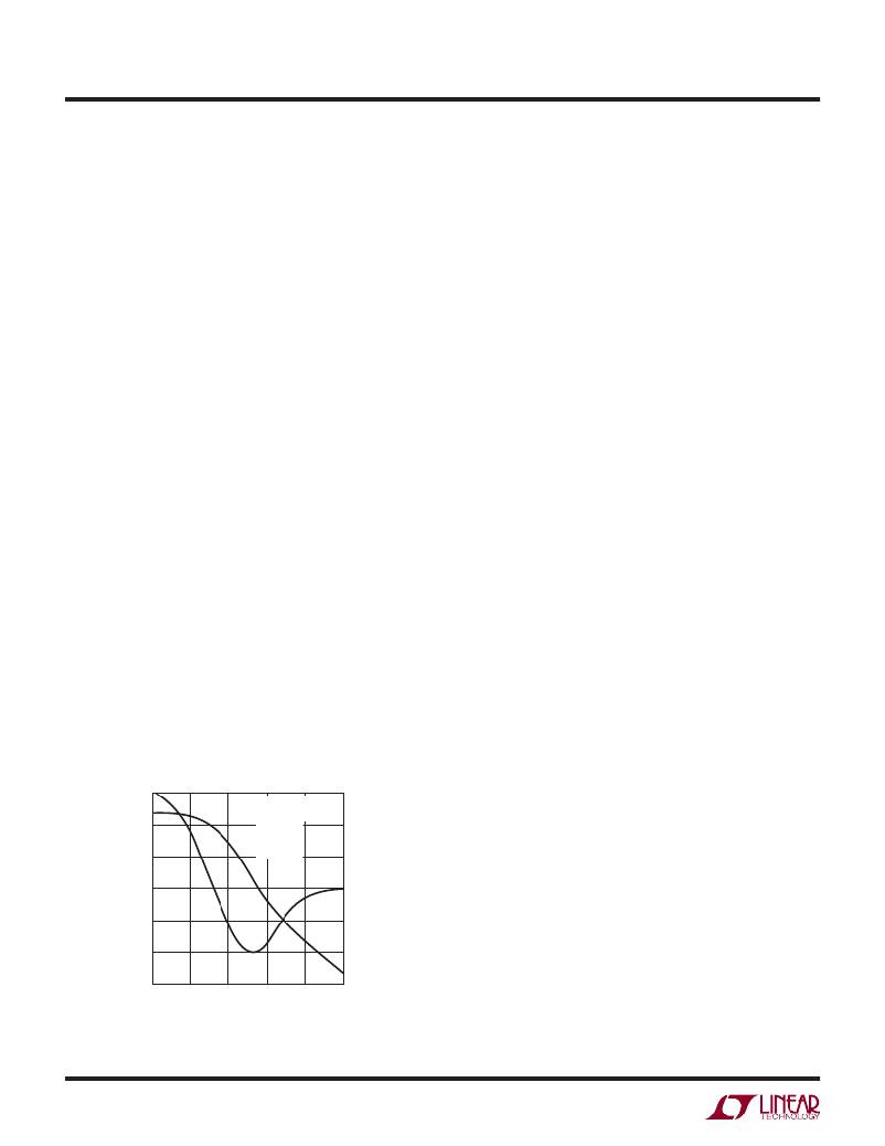
�Figure� 8� shows� the� overall� loop� response� with� a� 330pF� VC�
�capacitor� and� a� typical� 100μF� tantalum� output� capacitor.�
�The� response� is� set� by� the� following� terms:�
�Error� ampli?er:�
�DC� gain� set� by� g� m� and� R� L� =� 850μ� ?� 500k� =� 425.�
�Pole� set� by� C� F� and� R� L� =� (2π� ?� 500k� ?� 330p)� –1� =� 965Hz.�
�Unity-gain� set� by� C� F� and� g� m� =� (2π� ?� 330p� ?� 850μ� –1� )� –1� =�
�410kHz.�
�Power� stage:�
�DC� gain� set� by� g� m� and� R� L� (assume� 5Ω)� =� 5� ?� 5� =� 25.�
�Pole� set� by� C� OUT� and� R� L� =� (2π� ?� 100μ� ?� 10)� –1� =� 159Hz.�
�Unity-gain� set� by� C� OUT� and� g� m� =� (2π� ?� 100μ� ?� 5� –1� )� –1� =�
�8kHz.�
�Tantalum� output� capacitor:�
�Zero� set� by� C� OUT� and� C� ESR� =� (2π� ?� 100μ� ?� 0.1)� –1� =� 15.9kHz.�
�The� zero� produced� by� the� ESR� of� the� tantalum� output� capaci-�
�tor� is� very� useful� in� maintaining� stability.� Ceramic� output�
�capacitors� do� not� have� a� zero� due� to� very� low� ESR,� but� are�
�dominated� by� their� ESL.� They� form� a� notch� in� the� 1MHz� to�
�10MHz� range.� Without� this� zero,� the� V� C� pole� must� be� made�
�dominant.� A� typical� value� of� 2.2nF� will� achieve� this.�
�If� better� transient� response� is� required,� a� zero� can� be�
�added� to� the� loop� using� a� resistor� (R� C� )� in� series� with� the�
�compensation� capacitor.� As� the� value� of� R� C� is� increased,�
�transient� response� will� generally� improve,� but� two� effects�
�limit� its� value.� First,� the� combination� of� output� capacitor�
�ESR� and� a� large� R� C� may� stop� loop� gain� rolling� off� altogether.�
�Second,� if� the� loop� gain� is� not� rolled� suf?ciently� at� the�
�switching� frequency,� output� ripple� will� perturb� the� V� C� pin�
�enough� to� cause� unstable� duty� cycle� switching� similar�
�to� subharmonic� oscillation.� This� may� not� be� apparent�
�at� the� output.� Small� signal� analysis� will� not� show� this�
�since� a� continuous� time� system� is� assumed.� If� needed,�
�an� additional� capacitor� (C� F� )� can� be� added� to� the� V� C� pin� to�
�form� a� pole� at� typically� one� ?fth� the� switching� frequency�
�(If� R� C� =� ~� 5k,� C� F� =� ~� 100pF)�
�When� checking� loop� stability,� the� circuit� should� be� operated�
�over� the� application’s� full� voltage,� current� and� temperature�
�range.� Any� transient� loads� should� be� applied� and� the� output�
�voltage� monitored� for� a� well-damped� behavior.�
�CONVERTER� WITH� BACKUP� OUTPUT� REGULATOR�
�In� systems� with� a� primary� and� backup� supply,� for� example,�
�a� battery� powered� device� with� a� wall� adapter� input,� the�
�output� of� the� LT1765� can� be� held� up� by� the� backup� supply�
�with� its� input� disconnected.� In� this� condition,� the� SW� pin�
�will� source� current� into� the� V� IN� pin.� If� the� SHDN� pin� is� held�
�at� ground,� only� the� shutdown� current� of� 6μA� will� be� pulled�
�via� the� SW� pin� from� the� second� supply.� With� the� SHDN� pin�
�?oating,� the� LT1765� will� consume� its� quiescent� operating�
�current� of� 1mA.� The� V� IN� pin� will� also� source� current� to�
�any� other� components� connected� to� the� input� line.� If� this�
�load� is� greater� than� 10mA� or� the� input� could� be� shorted� to�
�ground,� a� series� Schottky� diode� must� be� added,� as� shown�
�in� Figure� 9.� With� these� safeguards,� the� output� can� be� held�
�at� voltages� up� to� the� V� IN� absolute� maximum� rating.�
�80�
�60�
�40�
�20�
�0�
�–20�
�V� OUT� =� 5V�
�C� OUT� =� 100μF,� 0.1Ω�
�C� C� =� 330pF�
�R� C� /C� F� =� 0�
�I� LOAD� =� 1A�
�PHASE�
�GAIN�
�180�
�150�
�120�
�90�
�60�
�30�
�BUCK� CONVERTER� WITH� ADJUSTABLE� SOFT-START�
�Large� capacitive� loads� or� high� input� voltages� can� cause�
�high� input� currents� at� start-up.� Figure� 10� shows� a� circuit�
�that� limits� the� dv/dt� of� the� output� at� start-up,� controlling�
�the� capacitor� charge� rate.� The� buck� converter� is� a� typical�
�con?guration� with� the� addition� of� R3,� R4,� C� SS� and� Q1.� As�
�the� output� starts� to� rise,� Q1� turns� on,� regulating� switch�
�current� via� the� V� C� pin� to� maintain� a� constant� dv/dt� at� the�
�output.� Output� rise� time� is� controlled� by� the� current� through�
�–40�
�10�
�100�
�1k� 10k�
�FREQUENCY� (Hz)�
�100k�
�0�
�1M�
�1765� F08�
�C� SS� de?ned� by� R4� and� Q1’s� V� BE� .� Once� the� output� is� in�
�regulation,� Q1� turns� off� and� the� circuit� operates� normally.�
�R3� is� transient� protection� for� the� base� of� Q1.�
�Figure� 8.� Overall� Loop� Response�
�1765fd�
�14�
�相关PDF资料 |
PDF描述 |
|---|---|
| HBM28DRKH | CONN EDGECARD 56POS DIP .156 SLD |
| MAX6715AUTLTD5+T | IC SUPERVISOR MPU SOT23-6 |
| GSM28DRST | CONN EDGECARD 56POS DIP .156 SLD |
| SC73-151 | INDUCTOR SMD 150UH 0.40A 1KHZ |
| EMM22DRKS | CONN EDGECARD 44POS DIP .156 SLD |
相关代理商/技术参数 |
参数描述 |
|---|---|
| LT1765EFE-3.3 | 功能描述:IC REG BUCK 3.3V 3A 16TSSOP RoHS:否 类别:集成电路 (IC) >> PMIC - 稳压器 - DC DC 开关稳压器 系列:- 设计资源:Design Support Tool 标准包装:1 系列:- 类型:升压(升压) 输出类型:固定 输出数:1 输出电压:3V 输入电压:0.75 V ~ 2 V PWM 型:- 频率 - 开关:- 电流 - 输出:100mA 同步整流器:是 工作温度:-40°C ~ 85°C 安装类型:表面贴装 封装/外壳:SOT-23-5 细型,TSOT-23-5 包装:剪切带 (CT) 供应商设备封装:TSOT-23-5 其它名称:AS1323-BTTT-30CT |
| LT1765EFE-3.3#PBF | 功能描述:IC REG BUCK 3.3V 3A 16TSSOP RoHS:是 类别:集成电路 (IC) >> PMIC - 稳压器 - DC DC 开关稳压器 系列:- 标准包装:250 系列:- 类型:降压(降压) 输出类型:固定 输出数:1 输出电压:1.2V 输入电压:2.05 V ~ 6 V PWM 型:电压模式 频率 - 开关:2MHz 电流 - 输出:500mA 同步整流器:是 工作温度:-40°C ~ 85°C 安装类型:表面贴装 封装/外壳:6-UFDFN 包装:带卷 (TR) 供应商设备封装:6-SON(1.45x1) 产品目录页面:1032 (CN2011-ZH PDF) 其它名称:296-25628-2 |
| LT1765EFE-3.3#PBF | 制造商:Linear Technology 功能描述:Switching Regulator IC |
| LT1765EFE-3.3#TR | 功能描述:IC REG BUCK 3.3V 3A 16TSSOP RoHS:否 类别:集成电路 (IC) >> PMIC - 稳压器 - DC DC 开关稳压器 系列:- 设计资源:Design Support Tool 标准包装:1 系列:- 类型:升压(升压) 输出类型:固定 输出数:1 输出电压:3V 输入电压:0.75 V ~ 2 V PWM 型:- 频率 - 开关:- 电流 - 输出:100mA 同步整流器:是 工作温度:-40°C ~ 85°C 安装类型:表面贴装 封装/外壳:SOT-23-5 细型,TSOT-23-5 包装:剪切带 (CT) 供应商设备封装:TSOT-23-5 其它名称:AS1323-BTTT-30CT |
| LT1765EFE-3.3#TRPBF | 功能描述:IC REG BUCK 3.3V 3A 16TSSOP RoHS:是 类别:集成电路 (IC) >> PMIC - 稳压器 - DC DC 开关稳压器 系列:- 设计资源:Design Support Tool 标准包装:1 系列:- 类型:升压(升压) 输出类型:固定 输出数:1 输出电压:3V 输入电压:0.75 V ~ 2 V PWM 型:- 频率 - 开关:- 电流 - 输出:100mA 同步整流器:是 工作温度:-40°C ~ 85°C 安装类型:表面贴装 封装/外壳:SOT-23-5 细型,TSOT-23-5 包装:剪切带 (CT) 供应商设备封装:TSOT-23-5 其它名称:AS1323-BTTT-30CT |
发布紧急采购,3分钟左右您将得到回复。