- 您现在的位置:买卖IC网 > PDF目录13897 > LT1765ES8#TR (Linear Technology)IC REG BUCK ADJ 3A 8SOIC PDF资料下载
参数资料
| 型号: | LT1765ES8#TR |
| 厂商: | Linear Technology |
| 文件页数: | 12/20页 |
| 文件大小: | 0K |
| 描述: | IC REG BUCK ADJ 3A 8SOIC |
| 标准包装: | 2,500 |
| 类型: | 降压(降压) |
| 输出类型: | 可调式 |
| 输出数: | 1 |
| 输出电压: | 1.2 V ~ 20 V |
| 输入电压: | 3 V ~ 25 V |
| PWM 型: | 电流模式 |
| 频率 - 开关: | 1.25MHz |
| 电流 - 输出: | 3A |
| 同步整流器: | 无 |
| 工作温度: | -40°C ~ 125°C |
| 安装类型: | 表面贴装 |
| 封装/外壳: | 8-SOIC(0.154",3.90mm 宽) |
| 包装: | 带卷 (TR) |
| 供应商设备封装: | 8-SOIC |
| 其它名称: | LT1765ES8TR LT1765ES8TR-ND |
�� �
�
�LT1765/LT1765-1.8/LT1765-2.5/�
�LT1765-3.3/LT1765-5�
�APPLICATIONS� INFORMATION�
�D2�
�MINIMIZE� D1,� C3�
�INPUT�
�CMDSH-3�
�LT1765� LOOP�
�15V�
�C3�
�4.7μF�
�CERAMIC�
�OFF� ON�
�V� IN�
�SHDN�
�SYNC�
�BOOST�
�LT1765-33�
�GND�
�C2�
�0.18μF�
�V� SW�
�FB�
�V� C�
�L1�
�2.7μH�
�OUTPUT�
�3.3V�
�2.5A�
�C1�
�VIN�
�D2�
�C2�
�C3�
�GND�
�C� C�
�KEEP� FB� AND� V� C�
�COMPONENTS� AND�
�TRACES� AWAY� FROM�
�HIGH� FREQUENCY,�
�HIGH� INPUT�
�COMPONENTS�
�C� C�
�D1�
�4.7μF�
�2.2nF�
�B220A�
�CERAMIC�
�L1�
�D1�
�1765� F06�
�VOUT�
�C1�
�GND�
�PLACE� FEEDTHROUGHS�
�UNDER� AND� AROUND�
�GROUND� PAD� FOR�
�GOOD� THERMAL�
�KELVIN�
�SENSE�
�V� OUT�
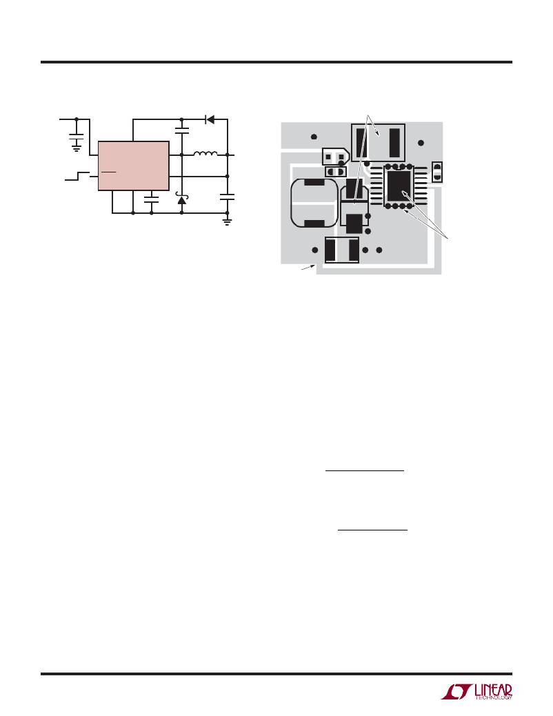
�Figure� 6.� Typical� Application� and� Layout� (Topside� Only� Shown)�
�1765� F6a�
�CONDUCTIVITY�
�rating.� A� ground� plane� should� always� be� used� under� the�
�switcher� circuitry� to� prevent� interplane� coupling� and�
�overall� noise.�
�The� V� C� and� FB� components� should� be� kept� as� far� away� as�
�possible� from� the� switch� and� boost� nodes.� The� LT1765�
�pinout� has� been� designed� to� aid� in� this.� The� ground� for�
�these� components� should� be� separated� from� the� switch�
�THERMAL� CALCULATIONS�
�Power� dissipation� in� the� LT1765� chip� comes� from� four�
�sources:� switch� DC� loss,� switch� AC� loss,� boost� circuit� cur-�
�rent,� and� input� quiescent� current.� The� following� formulas�
�show� how� to� calculate� each� of� these� losses.� These� formulas�
�assume� continuous� mode� operation,� so� they� should� not�
�be� used� for� calculating� ef?ciency� at� light� load� currents.�
�R� SW� (� I� OUT� )� (� V� OUT� )�
�current path. Failure to do so will result in poor stability�
�or� subharmonic� like� oscillation.�
�Board� layout� also� has� a� signi?cant� effect� on� thermal�
�resistance.� The� exposed� pad� or� GND� pin� is� a� continuous�
�Switch� loss:�
�P� SW� =�
�2�
�V� IN�
�+� 17� ns� (� I� OUT� )(� V� IN� )(� f� )�
�V� OUT� 2� (� I� OUT� /� 50� )�
�(� )�
�copper plate that runs under the LT1765 die. This is the�
�best� thermal� path� for� heat� out� of� the� package� as� can� be�
�seen� by� the� low� θ� JC� of� the� exposed� pad� package.� Reduc-�
�ing� the� thermal� resistance� from� Pin� 4� or� exposed� pad�
�onto� the� board� will� reduce� die� temperature� and� increase�
�the� power� capability� of� the� LT1765.� This� is� achieved� by�
�providing� as� much� copper� area� as� possible� around� this�
�pin/pad.� Also,� having� multiple� solder� ?lled� feedthroughs�
�to� a� continuous� copper� plane� under� LT1765� will� help� in�
�reducing� thermal� resistance.� Ground� plane� is� usually� suit-�
�able� for� this� purpose.� In� multilayer� PCB� designs,� placing� a�
�ground� plane� next� to� the� layer� with� the� LT1765� will� reduce�
�Boost� current� loss� for� VBOOST� =� VOUT:�
�P� BOOST� =�
�V� IN�
�Quiescent� current� loss:�
�P� Q� =� V� IN� 0� .� 001�
�R� SW� =� Switch� resistance� (≈0.13Ω� at� hot)�
�17ns� =� Equivalent� switch� current/voltage� overlap� time�
�f� =� Switch� frequency�
�thermal� resistance� to� a� minimum.�
�1765fd�
�12�
�相关PDF资料 |
PDF描述 |
|---|---|
| V300C24C150BF | CONVERTER MOD DC/DC 24V 150W |
| LTC3112EDHD#TRPBF | IC REG BUCK BST SYNC ADJ 16-DFN |
| RBA50DRMD-S288 | CONN EDGECARD 100POS .125 EXTEND |
| RMM08DTMI-S189 | CONN EDGECARD 16POS R/A .156 SLD |
| LTC3602EUF#TRPBF | IC REG BUCK SYNC ADJ 2.5A 20QFN |
相关代理商/技术参数 |
参数描述 |
|---|---|
| LT1766 | 制造商:LINER 制造商全称:Linear Technology 功能描述:1.4A, 500kHz Step-Down Switching Regulator |
| LT1766_1 | 制造商:LINER 制造商全称:Linear Technology 功能描述:5.5V to 60V 1.5A, 200kHz Step-Down Switching Regulator |
| LT1766-5 | 制造商:LINER 制造商全称:Linear Technology 功能描述:5.5V to 60V 1.5A, 200kHz Step-Down Switching Regulator |
| LT1766EFE | 功能描述:IC REG BUCK ADJ 1.5A 16TSSOP RoHS:否 类别:集成电路 (IC) >> PMIC - 稳压器 - DC DC 开关稳压器 系列:- 设计资源:Design Support Tool 标准包装:1 系列:- 类型:升压(升压) 输出类型:固定 输出数:1 输出电压:3V 输入电压:0.75 V ~ 2 V PWM 型:- 频率 - 开关:- 电流 - 输出:100mA 同步整流器:是 工作温度:-40°C ~ 85°C 安装类型:表面贴装 封装/外壳:SOT-23-5 细型,TSOT-23-5 包装:剪切带 (CT) 供应商设备封装:TSOT-23-5 其它名称:AS1323-BTTT-30CT |
| LT1766EFE#PBF | 功能描述:IC REG BUCK ADJ 1.5A 16TSSOP RoHS:是 类别:集成电路 (IC) >> PMIC - 稳压器 - DC DC 开关稳压器 系列:- 标准包装:250 系列:- 类型:降压(降压) 输出类型:固定 输出数:1 输出电压:1.2V 输入电压:2.05 V ~ 6 V PWM 型:电压模式 频率 - 开关:2MHz 电流 - 输出:500mA 同步整流器:是 工作温度:-40°C ~ 85°C 安装类型:表面贴装 封装/外壳:6-UFDFN 包装:带卷 (TR) 供应商设备封装:6-SON(1.45x1) 产品目录页面:1032 (CN2011-ZH PDF) 其它名称:296-25628-2 |
发布紧急采购,3分钟左右您将得到回复。