- 您现在的位置:买卖IC网 > PDF目录13879 > LT1766IFE-5 (Linear Technology)IC REG BUCK 5V 1.5A 16TSSOP PDF资料下载
参数资料
| 型号: | LT1766IFE-5 |
| 厂商: | Linear Technology |
| 文件页数: | 10/30页 |
| 文件大小: | 0K |
| 描述: | IC REG BUCK 5V 1.5A 16TSSOP |
| 标准包装: | 95 |
| 类型: | 降压(降压) |
| 输出类型: | 固定 |
| 输出数: | 1 |
| 输出电压: | 5V |
| 输入电压: | 5.5 V ~ 60 V |
| PWM 型: | 电流模式 |
| 频率 - 开关: | 200kHz |
| 电流 - 输出: | 1.5A |
| 同步整流器: | 无 |
| 工作温度: | -40°C ~ 125°C |
| 安装类型: | 表面贴装 |
| 封装/外壳: | 16-TSSOP(0.173",4.40mm)裸露焊盘 |
| 包装: | 管件 |
| 供应商设备封装: | 16-TSSOP-EP |
第1页第2页第3页第4页第5页第6页第7页第8页第9页当前第10页第11页第12页第13页第14页第15页第16页第17页第18页第19页第20页第21页第22页第23页第24页第25页第26页第27页第28页第29页第30页
�� �
�
�LT1766/LT1766-5�
�APPLICATIONS� INFORMATION�
�R� 2� (� V� OUT� ?� 1� .� 22� )�
�FEEDBACK PIN FUNCTIONS�
�The� feedback� (FB)� pin� on� the� LT1766� is� used� to� set� output�
�voltage� and� provide� several� overload� protection� features.�
�The� ?rst� part� of� this� section� deals� with� selecting� resistors�
�to� set� output� voltage� and� the� remaining� part� talks� about�
�foldback� frequency� and� current� limiting� created� by� the� FB�
�pin.� Please� read� both� parts� before� committing� to� a� ?nal�
�design.� The� 5V� ?xed� output� voltage� part� (LT1766-5)� has�
�internal� divider� resistors� and� the� FB� pin� is� renamed� SENSE,�
�connected� directly� to� the� output.�
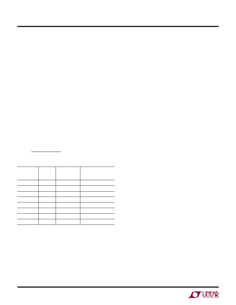
�The� suggested� value� for� the� output� divider� resistor� (see�
�Figure� 2)� from� FB� to� ground� (R2)� is� 5k� or� less,� and� a�
�formula� for� R1� is� shown� below.� The� output� voltage� error�
�caused� by� ignoring� the� input� bias� current� on� the� FB� pin�
�is� less� than� 0.25%� with� R2� =� 5k.� A� table� of� standard� 1%�
�values� is� shown� in� Table� 1� for� common� output� voltages.�
�Please� read� the� following� if� divider� resistors� are� increased�
�above� the� suggested� values.�
�R� 1� =�
�1� .� 22�
�Table� 1�
�regulator� to� operate� at� very� low� duty� cycles,� and� the�
�average� current� through� the� diode� and� inductor� is� equal�
�to� the� short-circuit� current� limit� of� the� switch� (typically� 2A�
�for� the� LT1766,� folding� back� to� less� than� 1A).� Minimum�
�switch� on-time� limitations� would� prevent� the� switcher�
�from� attaining� a� suf?ciently� low� duty� cycle� if� switching�
�frequency� were� maintained� at� 200kHz,� so� frequency� is�
�reduced� by� about� 5:1� when� the� feedback� pin� voltage� drops�
�below� 0.8V� (see� Frequency� Foldback� graph).� This� does�
�not� affect� operation� with� normal� load� conditions;� one�
�simply� sees� a� gear� shift� in� switching� frequency� during�
�start-up� as� the� output� voltage� rises.�
�In� addition� to� lower� switching� frequency,� the� LT1766� also�
�operates� at� lower� switch� current� limit� when� the� feedback�
�pin� voltage� drops� below� 0.6V.� Q2� in� Figure� 2� performs�
�this� function� by� clamping� the� V� C� pin� to� a� voltage� less� than�
�its� normal� 2.1V� upper� clamp� level.� This� foldback� current�
�limit� greatly� reduces� power� dissipation� in� the� IC,� diode�
�and� inductor� during� short-circuit� conditions.� External� syn-�
�chronization� is� also� disabled� to� prevent� interference� with�
�foldback� operation.� Again,� it� is� nearly� transparent� to� the� user�
�under� normal� load� conditions.� The� only� loads� that� may� be�
�affected� are� current� source� loads� which� maintain� full� load�
�OUTPUT�
�VOLTAGE�
�(V)�
�3�
�3.3�
�5�
�6�
�8�
�10�
�12�
�15�
�R2�
�(kΩ)�
�4.99�
�4.99�
�4.99�
�4.75�
�4.47�
�4.32�
�4.12�
�4.12�
�R1�
�(NEAREST� 1%)�
�(kΩ)�
�7.32�
�8.45�
�15.4�
�18.7�
�24.9�
�30.9�
�36.5�
�46.4�
�%� ERROR� AT� OUTPUT�
�DUE� TO� DISCREET� 1%�
�RESISTOR� STEPS�
�+0.32�
�–0.43�
�–0.30�
�+0.38�
�+0.20�
�–0.54�
�+0.24�
�–0.27�
�current� with� output� voltage� less� than� 50%� of� ?nal� value.�
�In� these� rare� situations� the� feedback� pin� can� be� clamped�
�above� 0.6V� with� an� external� diode� to� defeat� foldback� cur-�
�rent� limit.� Caution:� clamping� the� feedback� pin� means� that�
�frequency� shifting� will� also� be� defeated,� so� a� combination�
�of� high� input� voltage� and� dead� shorted� output� may� cause�
�the� LT1766� to� lose� control� of� current� limit.�
�The� internal� circuitry� which� forces� reduced� switching�
�frequency� also� causes� current� to� ?ow� out� of� the� feedback�
�pin� when� output� voltage� is� low.� The� equivalent� circuitry� is�
�shown� in� Figure� 2.� Q1� is� completely� off� during� normal� op-�
�More� Than� Just� Voltage� Feedback�
�The� feedback� pin� is� used� for� more� than� just� output� voltage�
�sensing.� It� also� reduces� switching� frequency� and� current�
�limit� when� output� voltage� is� very� low� (see� the� Frequency�
�Foldback� graph� in� Typical� Performance� Characteristics).�
�This� is� done� to� control� power� dissipation� in� both� the� IC�
�and� in� the� external� diode� and� inductor� during� short-cir-�
�cuit� conditions.� A� shorted� output� requires� the� switching�
�eration.� If� the� FB� pin� falls� below� 0.8V,� Q1� begins� to� conduct�
�current� and� reduces� frequency� at� the� rate� of� approximately�
�1.4kHz/μA.� To� ensure� adequate� frequency� foldback� (under�
�worst-case� short-circuit� conditions),� the� external� divider�
�Thevinin� resistance� must� be� low� enough� to� pull� 115μA� out�
�of� the� FB� pin� with� 0.44V� on� the� pin� (R� DIV� ≤� 3.8k).� The� net�
�result� is� that� reductions� in� frequency� and� current� limit� are�
�affected� by� output� voltage� divider� impedance.� Although�
�1766fc�
�10�
�相关PDF资料 |
PDF描述 |
|---|---|
| SC32-1R4 | INDUCTOR SMD 1.4UH 2.04A 7.96MHZ |
| GCM43DSUH | CONN EDGECARD 86POS DIP .156 SLD |
| EGM18DRMT | CONN EDGECARD 36POS .156 WW |
| LT3508HFE#TRPBF | IC REG BUCK ADJ 1.4A DL 16TSSOP |
| EMM12DRAI | CONN EDGECARD 24POS R/A .156 SLD |
相关代理商/技术参数 |
参数描述 |
|---|---|
| LT1766IFE-5#PBF | 功能描述:IC REG BUCK 5V 1.5A 16TSSOP RoHS:是 类别:集成电路 (IC) >> PMIC - 稳压器 - DC DC 开关稳压器 系列:- 设计资源:Design Support Tool 标准包装:1 系列:- 类型:升压(升压) 输出类型:固定 输出数:1 输出电压:3V 输入电压:0.75 V ~ 2 V PWM 型:- 频率 - 开关:- 电流 - 输出:100mA 同步整流器:是 工作温度:-40°C ~ 85°C 安装类型:表面贴装 封装/外壳:SOT-23-5 细型,TSOT-23-5 包装:剪切带 (CT) 供应商设备封装:TSOT-23-5 其它名称:AS1323-BTTT-30CT |
| LT1766IFE-5#TR | 功能描述:IC REG BUCK 5V 1.5A 16TSSOP RoHS:否 类别:集成电路 (IC) >> PMIC - 稳压器 - DC DC 开关稳压器 系列:- 设计资源:Design Support Tool 标准包装:1 系列:- 类型:升压(升压) 输出类型:固定 输出数:1 输出电压:3V 输入电压:0.75 V ~ 2 V PWM 型:- 频率 - 开关:- 电流 - 输出:100mA 同步整流器:是 工作温度:-40°C ~ 85°C 安装类型:表面贴装 封装/外壳:SOT-23-5 细型,TSOT-23-5 包装:剪切带 (CT) 供应商设备封装:TSOT-23-5 其它名称:AS1323-BTTT-30CT |
| LT1766IFE-5#TRPBF | 功能描述:IC REG BUCK 5V 1.5A 16TSSOP RoHS:是 类别:集成电路 (IC) >> PMIC - 稳压器 - DC DC 开关稳压器 系列:- 设计资源:Design Support Tool 标准包装:1 系列:- 类型:升压(升压) 输出类型:固定 输出数:1 输出电压:3V 输入电压:0.75 V ~ 2 V PWM 型:- 频率 - 开关:- 电流 - 输出:100mA 同步整流器:是 工作温度:-40°C ~ 85°C 安装类型:表面贴装 封装/外壳:SOT-23-5 细型,TSOT-23-5 包装:剪切带 (CT) 供应商设备封装:TSOT-23-5 其它名称:AS1323-BTTT-30CT |
| LT1766IFE-5-PBF | 制造商:LINER 制造商全称:Linear Technology 功能描述:5.5V to 60V 1.5A, 200kHz Step-Down Switching Regulator |
| LT1766IFE-5-TR | 制造商:LINER 制造商全称:Linear Technology 功能描述:5.5V to 60V 1.5A, 200kHz Step-Down Switching Regulator |
发布紧急采购,3分钟左右您将得到回复。