- 您现在的位置:买卖IC网 > PDF目录13917 > LT1766IGN#TR (Linear Technology)IC REG BUCK ADJ 1.5A 16SSOP PDF资料下载
参数资料
| 型号: | LT1766IGN#TR |
| 厂商: | Linear Technology |
| 文件页数: | 18/30页 |
| 文件大小: | 0K |
| 描述: | IC REG BUCK ADJ 1.5A 16SSOP |
| 标准包装: | 2,500 |
| 类型: | 降压(降压) |
| 输出类型: | 可调式 |
| 输出数: | 1 |
| 输出电压: | 1.2 V ~ 54 V |
| 输入电压: | 5.5 V ~ 60 V |
| PWM 型: | 电流模式 |
| 频率 - 开关: | 200kHz |
| 电流 - 输出: | 1.5A |
| 同步整流器: | 无 |
| 工作温度: | -40°C ~ 125°C |
| 安装类型: | 表面贴装 |
| 封装/外壳: | 16-SSOP(0.154",3.90mm 宽) |
| 包装: | 带卷 (TR) |
| 供应商设备封装: | 16-SSOP |
| 其它名称: | LT1766IGNTR |
第1页第2页第3页第4页第5页第6页第7页第8页第9页第10页第11页第12页第13页第14页第15页第16页第17页当前第18页第19页第20页第21页第22页第23页第24页第25页第26页第27页第28页第29页第30页
�� �
�
�LT1766/LT1766-5�
�APPLICATIONS� INFORMATION�
�Keep� the� connections� from� the� resistors� to� the� shutdown�
�pin� short� and� make� sure� that� interplane� or� surface� ca-�
�pacitance� to� the� switching� nodes� are� minimized.� If� high�
�resistor� values� are� used,� the� shutdown� pin� should� be�
�bypassed� with� a� 1000pF� capacitor� to� prevent� coupling�
�problems� from� the� switch� node.� If� hysteresis� is� desired�
�in� the� undervoltage� lockout� point,� a� resistor,� R� FB� ,� can�
�be� added� to� the� output� node.� Resistor� values� can� be�
�calculated� from:�
�compensation� used� to� prevent� subharmonic� switching� is�
�reduced.� This� type� of� subharmonic� switching� only� occurs�
�at� input� voltages� less� than� twice� output� voltage.� Higher�
�inductor� values� will� tend� to� eliminate� this� problem.� See�
�Frequency� Compensation� section� for� a� discussion� of� an�
�entirely� different� cause� of� subharmonic� switching� before�
�assuming� that� the� cause� is� insuf?cient� slope� compensa-�
�tion.� Application� Note� 19� has� more� details� on� the� theory�
�of� slope� compensation.�
�R� HI� =� R� LO� [� V� IN� ?� 2� .� 38� (� Δ� V� /� V� OUT� +� 1� )� +� Δ� V�
�2� .� 38� ?� R� LO� (� 5� .� 5� μ� A� )�
�R� FB� =� (� R� HI� )� (� V� OUT� /� Δ� V� )�
�25k� suggested� for� R� LO�
�]�
�At� power-up,� when� V� C� is� being� clamped� by� the� FB� pin� (see�
�Figure� 2,� Q2),� the� sync� function� is� disabled.� This� allows�
�the� frequency� foldback� to� operate� in� the� shorted� output�
�condition.� During� normal� operation,� switching� frequency� is�
�controlled� by� the� internal� oscillator� until� the� FB� pin� reaches�
�0.6V,� after� which� the� SYNC� pin� becomes� operational.� If� no�
�[� (� )� ]�
�2� .� 38� –� 25� k� (� )�
�(�
�)�
�V� IN� = Input voltage at which switching stops as input�
�voltage� descends� to� trip� level�
�Δ� V� =� Hysteresis� in� input� voltage� level�
�Example:� output� voltage� is� 5V,� switching� is� to� stop� if� input�
�voltage� drops� below� 12V� and� should� not� restart� unless� input�
�rises� back� to� 13.5V.� Δ� V� is� therefore� 1.5V� and� V� IN� =� 12V.�
�Let� R� LO� =� 25k.�
�25� k� 12� ?� 2� .� 38� 1� .� 5� /� 5� +� 1� +� 1� .� 5�
�R� HI� =�
�5� .� 5� μ� A�
�=� 25� k� (� 10� .� 41� )� =� 116� k�
�2� .� 24�
�R� FB� =� 116� k� 5� /� 1� .� 5� =� 387� k�
�SYNCHRONIZING�
�The� SYNC� input� must� pass� from� a� logic� level� low,� through�
�synchronization� is� required,� this� pin� should� be� connected�
�to� ground.�
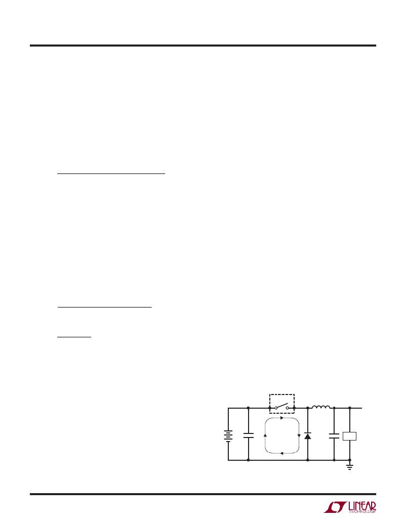
�LAYOUT� CONSIDERATIONS�
�As� with� all� high� frequency� switchers,� when� considering�
�layout,� care� must� be� taken� in� order� to� achieve� optimal�
�electrical,� thermal� and� noise� performance.� For� maxi-�
�mum� ef?ciency,� switch� rise� and� fall� times� are� typically�
�in� the� nanosecond� range.� To� prevent� noise� both� radiated�
�and� conducted,� the� high� speed� switching� current� path,�
�shown� in� Figure� 5,� must� be� kept� as� short� as� possible.�
�This� is� implemented� in� the� suggested� layout� of� Figure� 6.�
�Shortening� this� path� will� also� reduce� the� parasitic� trace�
�inductance� of� approximately� 25nH/inch.� At� switch� off,� this�
�parasitic� inductance� produces� a� ?yback� spike� across� the�
�LT1766� switch.� When� operating� at� higher� currents� and�
�input� voltages,� with� poor� layout,� this� spike� can� generate�
�voltages� across� the� LT1766� that� may� exceed� its� absolute�
�the� maximum� synchronization� threshold� with� a� duty� cycle�
�between� 10%� and� 90%.� The� input� can� be� driven� directly�
�LT1766�
�L1�
�5V�
�from� a� logic� level� output.� The� synchronizing� range� is� equal�
�to� initial� operating� frequency� up� to� 700kHz.� This� means�
�HIGH�
�that� minimum� practical� sync� frequency� is� equal� to� the�
�worst-case� high� self-oscillating� frequency� (228kHz),� not�
�V� IN�
�C3�
�FREQUENCY�
�CIRCULATING�
�PATH�
�D1� C1�
�LOAD�
�the� typical� operating� frequency� of� 200kHz.� Caution� should�
�be� used� when� synchronizing� above� 265kHz� because� at�
�higher� sync� frequencies� the� amplitude� of� the� internal� slope�
�Figure� 5.� High� Speed� Switching� Path�
�1766� F05�
�1766fc�
�18�
�相关PDF资料 |
PDF描述 |
|---|---|
| RGM10DTBN | CONN EDGECARD 20POS R/A .156 SLD |
| MAX6720AUTTZD5+T | IC SUPERVISOR MPU SOT23-6 |
| MAX6720AUTVDD2+T | IC SUPERVISOR MPU SOT23-6 |
| RSM10DTBH | CONN EDGECARD 20POS R/A .156 SLD |
| RMM10DTBH | CONN EDGECARD 20POS R/A .156 SLD |
相关代理商/技术参数 |
参数描述 |
|---|---|
| LT1766IGN-TRPBF | 制造商:LINER 制造商全称:Linear Technology 功能描述:5.5V to 60V 1.5A, 200kHz Step-Down Switching Regulator |
| LT1767 | 制造商:LINER 制造商全称:Linear Technology 功能描述:1.4A, 500kHz Step-Down Switching Regulator |
| LT1767-1.8 | 制造商:LINER 制造商全称:Linear Technology 功能描述:Monolithic 1.5A, 1.25MHz Step-Down Switching Regulators |
| LT1767-2.5 | 制造商:LINER 制造商全称:Linear Technology 功能描述:Monolithic 1.5A, 1.25MHz Step-Down Switching Regulators |
| LT1767-3.3 | 制造商:LINER 制造商全称:Linear Technology 功能描述:Monolithic 1.5A, 1.25MHz Step-Down Switching Regulators |
发布紧急采购,3分钟左右您将得到回复。