参数资料
| 型号: | LT1777IS#TRPBF |
| 厂商: | Linear Technology |
| 文件页数: | 9/24页 |
| 文件大小: | 0K |
| 描述: | IC REG BUCK ADJ 0.7A 16SOIC |
| 标准包装: | 2,500 |
| 类型: | 降压(降压) |
| 输出类型: | 可调式 |
| 输出数: | 1 |
| 输出电压: | 1.24 V ~ 30 V |
| 输入电压: | 12 V ~ 48 V |
| PWM 型: | 电流模式 |
| 频率 - 开关: | 100kHz |
| 电流 - 输出: | 700mA |
| 同步整流器: | 无 |
| 工作温度: | -40°C ~ 125°C |
| 安装类型: | 表面贴装 |
| 封装/外壳: | 16-SOIC(0.154",3.90mm 宽) |
| 包装: | 带卷 (TR) |
| 供应商设备封装: | 16-SOIC |
�� �
�
�LT1777�
�APPLICATIO� N� S� I� N� FOR� M� ATIO� N�
�Basics� of� Low� Noise� Operation�
�Switching� power� supply� circuits� are� often� preferred� over�
�linear� topologies� for� their� improved� efficiency� (P� OUT� /� P� IN� ).�
�However,� their� typically� rapid� voltage� and� current� slew�
�rates� often� cause� “radio� frequency”� interference� prob-�
�lems,� commonly� referred� to� as� “RFI”.� The� LT1777� is�
�designed� to� provide� a� less� aggressive� voltage� slew� rate�
�and� a� user-programmable� current� slew� rate� to� eliminate�
�the� highest� frequency� harmonics� of� RFI� emissions.� These�
�highest� frequency� components� are� typically� the� most�
�troublesome.� Optimum� behavior� is� obtained� by� a� combi-�
�nation� of� proper� circuit� design,� which� includes� passive�
�component� selection,� and� proper� printed� circuit� board�
�layout� technique.�
�There� are� two� types� of� RFI� emissions,� i.e.,� conducted� and�
�radiated.� Conducted� interference� travels� directly� through�
�“wires”,� as� opposed� to� radiated� interference,� which� travels�
�through� the� air.� Conducted� RFI� can� be� created� by� a�
�switching� power� supply� at� its� input� voltage� supply� node,�
�its� output� node(s)� or� both.� It� is� typically� caused� by� pulsatile�
�current� flow� through� the� residual� high� frequency� imped-�
�ance� (ESR)� of� bypass� capacitors.�
�Radiated� interference� can� be� of� two� types:� electric� (E� field)�
�or� magnetic� (B� field).� E� field� interference� is� caused� by� stray�
�capacitance� coupling� of� the� node(s)� which� swing� rapidly�
�over� a� large� voltage� excursion.� In� the� LT1777,� this� in-�
�external� sense� inductor� to� set� a� maximum� allowed� dI/dt�
�rate.� This� attenuates� the� highest� frequency� components� of�
�generated� B� field� RFI.� Minimal� lead� length� in� the� path� is�
�also� essential� to� minimize� generated� RFI.�
�A� second� potential� source� of� magnetic� RFI� is� the� main�
�(power)� inductor.� Fortunately,� the� natural� triangular� be-�
�havior� of� the� current� waveform� in� the� main� inductor� tends�
�to� generate� magnetic� field� energy� concentrated� in� the�
�fundamental� and� lower� harmonics.� Nevertheless,� the� rela-�
�tively� intense� magnetic� field� present� in� the� main� inductor�
�can� cause� coupling� problems,� especially� if� the� main� induc-�
�tor� is� of� an� open� construction� type.� So� called� rod� or� barrel�
�inductors� may� be� the� physically� smallest� and� most� effec-�
�tive� types,� but� their� magnetic� field� extends� far� beyond� the�
�device� itself.� Closed� type� inductors,� toroids� for� example,�
�contain� the� magnetic� field� nearly� completely.� These� are�
�generally� preferred� for� low� noise� behavior.�
�The� sense� inductor� sees� a� much� more� rapid� current� slew�
�rate� than� does� the� main� inductor.� However� the� sense�
�inductor� is� physically� smaller� and� of� much� lower� induc-�
�tance� than� the� main� inductor.� These� factors� tend� to� reduce�
�its� propensity� to� generate� magnetic� interference� prob-�
�lems.� Nevertheless,� more� sensitive� applications� can� opt�
�for� a� closed� type� magnetic� construction� on� the� sense�
�inductor.�
�cludes� the� V� SW� and� V� D� nodes.� E� field� radiation� is� kept� low�
�by� minimizing� the� length� and� area� of� all� traces� connected�
�to� these� nodes.� A� ground� plane� should� always� be� used�
�under� the� switcher� circuitry� to� prevent� interplane� cou-�
�pling.� Although� these� nodes� swing� over� a� voltage� range�
�roughly� equal� to� the� input� voltage,� the� limited� dV/dt� rate� of�
�V� IN�
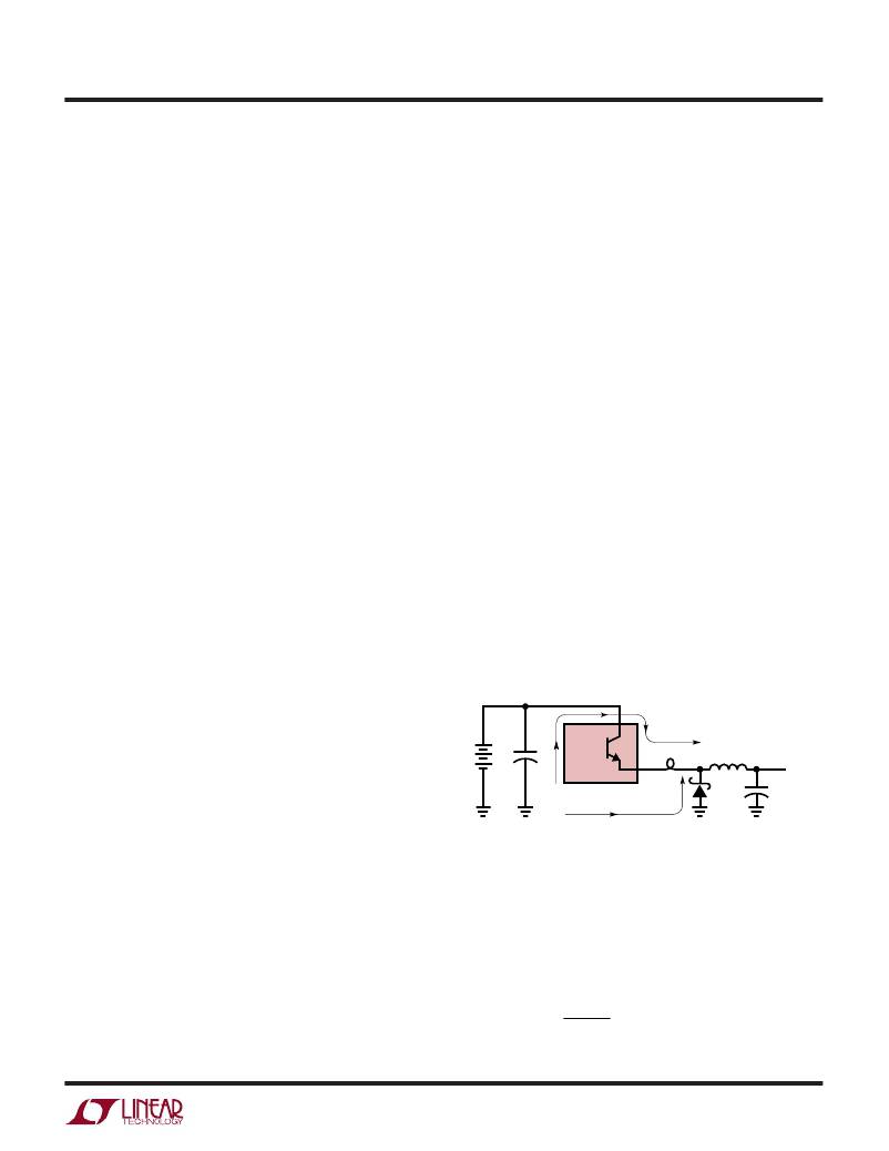
�+�
�C1�
�LT1777�
�L� SENSE�
�L� MAIN�
�D1�
�+�
�V� OUT�
�C2�
�1777� F01�
�the� LT1777� reduces� the� highest� frequency� components� of�
�the� generated� E� field� RFI.�
�B� field� RFI� is� simply� coupling� of� high� frequency� magnetic�
�fields� generated� by� the� offending� circuitry.� High� frequency�
�magnetic� fields� are� created� by� relatively� rapidly� changing�
�currents,� and� the� high� speed� current� switching� path� in� the�
�LT1777� is� shown� schematically� in� Figure� 1.� This� includes�
�Figure� 1.� High� Speed� Current� Switching� Paths�
�Selecting� Sense� Inductor�
�The� LT1777� uses� an� external� sense� inductor� to� set� a�
�theoretical� limit� for� current� ramp� rate� according� to� the�
�formula:�
�the� input� capacitor,� output� switch,� sense� inductor� and�
�output� diode.� Normal� switching� supply� operation� requires�
�a� rapid� switching� of� current� back� and� forth� between� the�
�Max� dI� /� dt� =�
�2� V� BE�
�L� SENSE�
�output� switch� and� output� diode.� The� LT1777� uses� the�
�9�
�相关PDF资料 |
PDF描述 |
|---|---|
| LT1786FCS#TR | IC REG SW CCFL SMBUS PROG 16SOIC |
| LT1912EMSE#TRPBF | IC REG BUCK ADJ 2A 10MSOP |
| LT1913IDD#TRPBF | IC REG BUCK ADJ 3.5A 10DFN |
| LT1930AES5#TRM | IC REG BOOST ADJ 1A TSOT23-5 |
| LT1931AIS5#TRPBF | IC REG INV 1A TSOT23-5 |
相关代理商/技术参数 |
参数描述 |
|---|---|
| LT1780 | 制造商:LINER 制造商全称:Linear Technology 功能描述:Low Power 5V RS232 Dual Driver/Receiver with 【15kV ESD Protection |
| LT17801IN | 制造商:未知厂家 制造商全称:未知厂家 功能描述:Transceiver |
| LT1780CN | 功能描述:IC DVR/RCVR 5V RS232 DUAL 18-DIP RoHS:否 类别:集成电路 (IC) >> 接口 - 驱动器,接收器,收发器 系列:- 标准包装:27 系列:- 类型:收发器 驱动器/接收器数:3/3 规程:RS232,RS485 电源电压:4.75 V ~ 5.25 V 安装类型:表面贴装 封装/外壳:28-SOIC(0.295",7.50mm 宽) 供应商设备封装:28-SOIC 包装:管件 |
| LT1780CN#PBF | 功能描述:IC DVR/RCVR 5V RS232 DUAL 18-DIP RoHS:是 类别:集成电路 (IC) >> 接口 - 驱动器,接收器,收发器 系列:- 产品培训模块:RS-232 & USB Transceiver 标准包装:2,000 系列:- 类型:收发器 驱动器/接收器数:1/1 规程:RS232 电源电压:3 V ~ 5.5 V 安装类型:表面贴装 封装/外壳:16-SSOP(0.209",5.30mm 宽) 供应商设备封装:16-SSOP 包装:带卷 (TR) 其它名称:296-19849-2 |
| LT1780CSW | 功能描述:IC DVR/RCVR 5V RS232 DUAL 18SOIC RoHS:否 类别:集成电路 (IC) >> 接口 - 驱动器,接收器,收发器 系列:- 标准包装:27 系列:- 类型:收发器 驱动器/接收器数:3/3 规程:RS232,RS485 电源电压:4.75 V ~ 5.25 V 安装类型:表面贴装 封装/外壳:28-SOIC(0.295",7.50mm 宽) 供应商设备封装:28-SOIC 包装:管件 |
发布紧急采购,3分钟左右您将得到回复。