- 您现在的位置:买卖IC网 > PDF目录5902 > LT1789IS8-1#TRPBF (Linear Technology)IC INSTRUMENT AMP R-R OUT 8-SOIC PDF资料下载
参数资料
| 型号: | LT1789IS8-1#TRPBF |
| 厂商: | Linear Technology |
| 文件页数: | 24/24页 |
| 文件大小: | 0K |
| 描述: | IC INSTRUMENT AMP R-R OUT 8-SOIC |
| 标准包装: | 2,500 |
| 放大器类型: | 仪表 |
| 电路数: | 1 |
| 转换速率: | 0.026 V/µs |
| 增益带宽积: | 60kHz |
| 电流 - 输入偏压: | 17nA |
| 电压 - 输入偏移: | 30µV |
| 电流 - 电源: | 85µA |
| 电流 - 输出 / 通道: | 8.5mA |
| 电压 - 电源,单路/双路(±): | 2.2 V ~ 36 V,±1.1 V ~ 18 V |
| 工作温度: | -40°C ~ 85°C |
| 安装类型: | 表面贴装 |
| 封装/外壳: | 8-SOIC(0.154",3.90mm 宽) |
| 供应商设备封装: | 8-SO |
| 包装: | 带卷 (TR) |
LT1789-1/LT1789-10
9
1789fc
Note 1: Stresses beyond those listed under Absolute Maximum Ratings
may cause permanent damage to the device. Exposure to any Absolute
Maximum Rating condition for extended periods may affect device
reliability and lifetime.
Note 2: Does not include the effect of the external gain resistor RG.
Note 3: This parameter is not 100% tested.
Note 4: The LT1789C-1/ LT1789C-10 is guaranteed to meet specified
performance from 0°C to 70°C and is designed, characterized and
expected to meet these extended temperature limits, but is not tested at
–40°C and 85°C. The LT1789I-1/ LT1789I-10 is guaranteed to meet the
extended temperature limits.
SYMBOL PARAMETER
CONDITIONS
LT1789-1
LT1789-10
UNITS
MIN
TYP
MAX
MIN
TYP
MAX
PSRR
Power Supply Rejection Ratio
LT1789-1, VS = ±1.25V to ±16V
LT1789-10, VS = ±1.50V to ±16V
G = 1
G = 10
G = 100, 1000
l
90
100
102
96
102
dB
Minimum Supply Voltage
l
±1.25
±1.50
V
IS
Supply Current
l
160
A
VO
Output Voltage Swing
l ±14.15
±14.15
V
SR
Slew Rate
VOUT = ±10V
l
0.008
0.024
V/s
ELECTRICAL CHARACTERISTICS The l denotes the specifications which apply over the temperature range of
–40°C ≤ TA ≤ 85°C. VS = ±15V, RL = 20k, VCM = VREF = 0V, unless otherwise noted. (Note 4)
Note 5: Hysteresis in offset voltage is created by package stress that
differs depending on whether the IC was previously at a higher or lower
temperature. Offset voltage hysteresis is always measured at 25°C, but
the IC is cycled to 85°C I-grade (or 70°C C-grade) or – 40°C I-grade
(0°C C-grade) before successive measurement. 60% of the parts will
pass the typical limit on the data sheet.
Note 6: VS = 5V limits are guaranteed by correlation to VS = 3V and
VS = ±15V tests.
Note 7: VS = 3V limits are guaranteed by correlation to VS = 5V and
VS = ±15V tests.
Note 8: This parameter is not tested at VS = 3V on the LT1789-10 due
to an increase in sensitivity to test system noise. Actual performance is
expected to be similar to performance at VS = 5V.
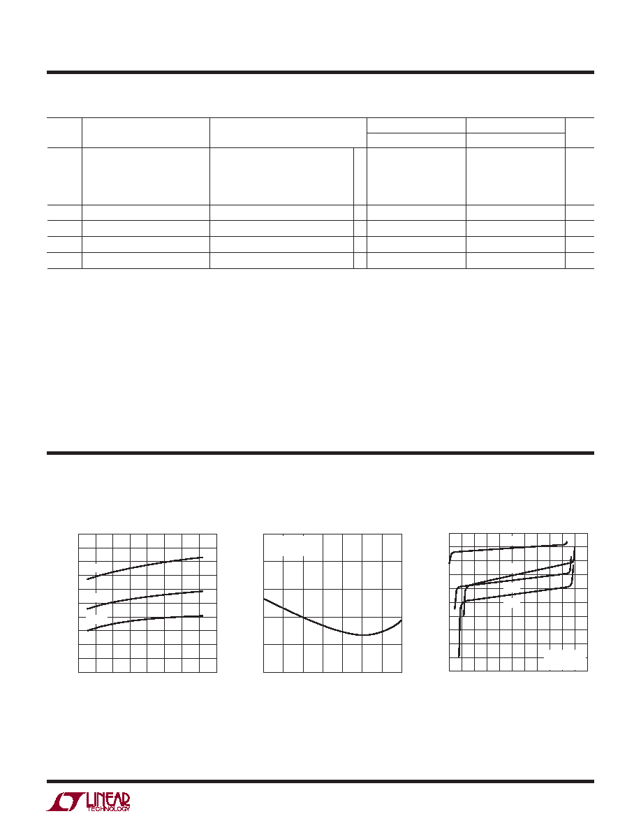
TYPICAL PERFORMANCE CHARACTERISTICS
Supply Current vs Supply Voltage
Input Bias Current
vs Temperature
Input Bias Current
vs Common Mode Input Voltage
TOTAL SUPPLY VOLTAGE (V)
0
20
SUPPLY
CURRENT
(μA)
30
50
60
70
120
90
10
20
25
1789 G01
40
100
110
80
515
30
35
40
125°C
25°C
–55°C
TEMPERATURE (°C)
–50
–25
INPUT
BIAS
CURRENT
(nA)
–15
0
50
75
1789 G02
–20
–5
–10
25
100
125
VS = 5V, 0V
VCM = 2.5V
COMMON MODE INPUT VOLTAGE (V)
0
INPUT
BIAS
CURRENT
(nA)
–18
–14
–10
4.5
1789 G03
–22
–26
–20
–16
–12
–24
–28
–30
1.5
2.5
3.5
1
0.5
–0.5
5
2
3
4
VS = 5V, 0V
VREF = 2.5V
–55°C
125°C
25°C
85°C
(LT1789-1, LT1789-10)
相关PDF资料 |
PDF描述 |
|---|---|
| TSW-139-06-G-D | CONN HEADER 78POS .100" DL GOLD |
| 77313-801-14LF | CONN HEADER .100 DUAL STR 14POS |
| TSW-139-05-G-D | CONN HEADER 78POS .100" DL GOLD |
| TSW-143-14-G-D | CONN HEADER 86POS .100" DL GOLD |
| 57102-G08-02 | MINITEK UNSHRD HDR S-TRAIGHT |
相关代理商/技术参数 |
参数描述 |
|---|---|
| LT1790 | 制造商:LINER 制造商全称:Linear Technology 功能描述:Easy-to-Use, Ultra-Tiny, Differential, 16-Bit ADC With I2C Interface |
| LT1790-2.5 | 制造商:LINER 制造商全称:Linear Technology 功能描述:Serial 12-Bit/14-Bit, 2.8Msps |
| LT1790A | 制造商:LINER 制造商全称:Linear Technology 功能描述:Micropower SOT-23 Low Dropout Reference Family |
| LT1790A-2.5 | 制造商:LINER 制造商全称:Linear Technology 功能描述:Dual Current Output 12-/14-/16-Bit SoftSpan DACs with Parallel I/O |
| LT1790AC | 制造商:LINER 制造商全称:Linear Technology 功能描述:Micropower SOT-23 Low Dropout Reference Family |
发布紧急采购,3分钟左右您将得到回复。