参数资料
| 型号: | LT1912EMSE#TRPBF |
| 厂商: | Linear Technology |
| 文件页数: | 13/24页 |
| 文件大小: | 0K |
| 描述: | IC REG BUCK ADJ 2A 10MSOP |
| 标准包装: | 2,500 |
| 类型: | 降压(降压) |
| 输出类型: | 可调式 |
| 输出数: | 1 |
| 输出电压: | 0.79 V ~ 20 V |
| 输入电压: | 3.6 V ~ 36 V |
| PWM 型: | 电流模式 |
| 频率 - 开关: | 200kHz ~ 500kHz |
| 电流 - 输出: | 2A |
| 同步整流器: | 无 |
| 工作温度: | -40°C ~ 125°C |
| 安装类型: | 表面贴装 |
| 封装/外壳: | 10-TFSOP,10-MSOP(0.118",3.00mm 宽)裸露焊盘 |
| 包装: | 带卷 (TR) |
| 供应商设备封装: | 10-MSOP |
�� �
�
�LT1912�
�APPLICATIONS� INFORMATION�
�g� m� =� 3.5mho�
�ESR�
�C1�
�+�
�V� C�
�GND�
�10μs/DIV�
�andinparticularthetypeofoutputcapacitor.Apractical�
�approach� is� to� start� with� one� of� the� circuits� in� this� data�
�sheet� that� is� similar� to� your� application� and� tune� the� com-�
�pensation� network� to� optimize� the� performance.� Stability�
�should� then� be� checked� across� all� operating� conditions,�
�including� load� current,� input� voltage� and� temperature.� The�
�LT1375� data� sheet� contains� a� more� thorough� discussion� of�
�loop� compensation� and� describes� how� to� test� the� stabil-�
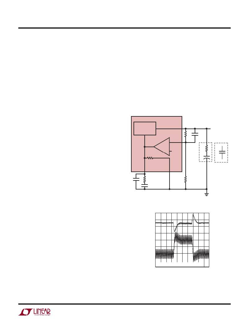
�ity� using� a� transient� load.� Figure� 2� shows� an� equivalent�
�circuit� for� the� LT1912� control� loop.� The� error� amplifier� is� a�
�transconductance� amplifier� with� finite� output� impedance.�
�The� power� section,� consisting� of� the� modulator,� power�
�switch� and� inductor,� is� modeled� as� a� transconductance�
�amplifier� generating� an� output� current� proportional� to�
�the� voltage� at� the� V� C� pin.� Note� that� the� output� capacitor�
�integrates� this� current,� and� that� the� capacitor� on� the� V� C� pin�
�(C� C� )� integrates� the� error� amplifier� output� current,� resulting�
�in� two� poles� in� the� loop.� In� most� cases� a� zero� is� required�
�and� comes� from� either� the� output� capacitor� ESR� or� from�
�a� resistor� R� C� in� series� with� C� C� .� This� simple� model� works�
�well� as� long� as� the� value� of� the� inductor� is� not� too� high�
�and� the� loop� crossover� frequency� is� much� lower� than� the�
�switching� frequency.� A� phase� lead� capacitor� (C� PL� )� across�
�the� feedback� divider� may� improve� the� transient� response.�
�Figure� 3� shows� the� transient� response� when� the� load� current�
�is� stepped� from� 500mA� to� 1500mA� and� back� to� 500mA.�
�BOOST� and� BIAS� Pin� Considerations�
�Capacitor� C3� and� the� internal� boost� Schottky� diode� (see�
�the� Block� Diagram)� are� used� to� generate� a� boost� volt-�
�age� that� is� higher� than� the� input� voltage.� In� most� cases�
�a� 0.22μF� capacitor� will� work� well.� Figure� 2� shows� three�
�ways� to� arrange� the� boost� circuit.� The� BOOST� pin� must� be�
�more� than� 2.3V� above� the� SW� pin� for� best� efficiency.� For�
�outputs� of� 3V� and� above,� the� standard� circuit� (Figure� 4a)�
�is� best.� For� outputs� between� 2.8V� and� 3V,� use� a� 1μF� boost�
�capacitor.� A� 2.5V� output� presents� a� special� case� because� it�
�is� marginally� adequate� to� support� the� boosted� drive� stage�
�while� using� the� internal� boost� diode.� For� reliable� BOOST� pin�
�operation� with� 2.5V� outputs� use� a� good� external� Schottky�
�diode� (such� as� the� ON� Semi� MBR0540),� and� a� 1μF� boost�
�capacitor� (see� Figure� 4b).� For� lower� output� voltages� the�
�boost� diode� can� be� tied� to� the� input� (Figure� 4c),� or� to�
�another� supply� greater� than� 2.8V.� Tying� BD� to� V� IN� reduces�
�the� maximum� input� voltage� to� 30V.� The� circuit� in� Figure� 4a�
�is� more� efficient� because� the� BOOST� pin� current� and� BD�
�pin� quiescent� current� comes� from� a� lower� voltage� source.�
�You� must� also� be� sure� that� the� maximum� voltage� ratings�
�of� the� BOOST� and� BD� pins� are� not� exceeded.�
�The� minimum� operating� voltage� of� an� LT1912� application�
�is� limited� by� the� minimum� input� voltage� (3.6V)� and� by� the�
�maximum� duty� cycle� as� outlined� in� a� previous� section.� For�
�proper� startup,� the� minimum� input� voltage� is� also� limited�
�by� the� boost� circuit.� If� the� input� voltage� is� ramped� slowly,�
�then� the� boost� capacitor� may� not� be� fully� charged.� Because�
�LT1912�
�CURRENT� MODE� SW�
�POWER� STAGE� OUTPUT�
�ERROR�
�AMPLIFIER� R1� C� PL�
�FB�
�g� m� =�
�420μmho�
�0.8V�
�3Meg�
�C1�
�POLYMER� CERAMIC�
�OR�
�TANTALUM�
�C� F� R� C� R2�
�C� C�
�1912� F02�
�Figure� 2.� Model� for� Loop� Response�
�V� OUT�
�100mV/DIV�
�I� L�
�0.5A/DIV�
�V� IN� =� 12V;� FRONT� PAGE� APPLICATION�
�1912� F03�
�Figure� 3.� Transient� Load� Response� of� the� LT1912� Front� Page�
�Application� as� the� Load� Current� is� Stepped� from� 500mA� to�
�1500mA.� V� OUT� =� 3.3V�
�1912fa�
�13�
�相关PDF资料 |
PDF描述 |
|---|---|
| LT1913IDD#TRPBF | IC REG BUCK ADJ 3.5A 10DFN |
| LT1930AES5#TRM | IC REG BOOST ADJ 1A TSOT23-5 |
| LT1931AIS5#TRPBF | IC REG INV 1A TSOT23-5 |
| LT1933HS6#TRMPBF | IC REG BUCK ADJ 0.6A TSOT23-6 |
| LT1934IDCB-1#TRPBF | IC REG BUCK ADJ 60MA 6DFN |
相关代理商/技术参数 |
参数描述 |
|---|---|
| LT1913 | 制造商:LINER 制造商全称:Linear Technology 功能描述:25V, 3.5A, 2.4MHz Step-Down Switching Regulator |
| LT1913EDD#PBF | 功能描述:IC REG BUCK ADJ 3.5A 10DFN RoHS:是 类别:集成电路 (IC) >> PMIC - 稳压器 - DC DC 开关稳压器 系列:- 标准包装:250 系列:- 类型:降压(降压) 输出类型:固定 输出数:1 输出电压:1.2V 输入电压:2.05 V ~ 6 V PWM 型:电压模式 频率 - 开关:2MHz 电流 - 输出:500mA 同步整流器:是 工作温度:-40°C ~ 85°C 安装类型:表面贴装 封装/外壳:6-UFDFN 包装:带卷 (TR) 供应商设备封装:6-SON(1.45x1) 产品目录页面:1032 (CN2011-ZH PDF) 其它名称:296-25628-2 |
| LT1913EDD#TRPBF | 功能描述:IC REG BUCK ADJ 3.5A 10DFN RoHS:是 类别:集成电路 (IC) >> PMIC - 稳压器 - DC DC 开关稳压器 系列:- 设计资源:Design Support Tool 标准包装:1 系列:- 类型:升压(升压) 输出类型:固定 输出数:1 输出电压:3V 输入电压:0.75 V ~ 2 V PWM 型:- 频率 - 开关:- 电流 - 输出:100mA 同步整流器:是 工作温度:-40°C ~ 85°C 安装类型:表面贴装 封装/外壳:SOT-23-5 细型,TSOT-23-5 包装:剪切带 (CT) 供应商设备封装:TSOT-23-5 其它名称:AS1323-BTTT-30CT |
| LT1913EDD-PBF | 制造商:LINER 制造商全称:Linear Technology 功能描述:25V, 3.5A, 2.4MHz Step-Down Switching Regulator |
| LT1913EDD-TRPBF | 制造商:LINER 制造商全称:Linear Technology 功能描述:25V, 3.5A, 2.4MHz Step-Down Switching Regulator |
发布紧急采购,3分钟左右您将得到回复。