- 您现在的位置:买卖IC网 > PDF目录14805 > LT1913EDD#PBF (Linear Technology)IC REG BUCK ADJ 3.5A 10DFN PDF资料下载
参数资料
| 型号: | LT1913EDD#PBF |
| 厂商: | Linear Technology |
| 文件页数: | 15/24页 |
| 文件大小: | 0K |
| 描述: | IC REG BUCK ADJ 3.5A 10DFN |
| 标准包装: | 121 |
| 类型: | 降压(降压) |
| 输出类型: | 可调式 |
| 输出数: | 1 |
| 输出电压: | 0.79 V ~ 25 V |
| 输入电压: | 3.6 V ~ 25 V |
| PWM 型: | 电流模式 |
| 频率 - 开关: | 200kHz ~ 2.4MHz |
| 电流 - 输出: | 3.5A |
| 同步整流器: | 无 |
| 工作温度: | -40°C ~ 125°C |
| 安装类型: | 表面贴装 |
| 封装/外壳: | 10-WFDFN 裸露焊盘 |
| 包装: | 管件 |
| 供应商设备封装: | 10-DFN(3x3) |
| 产品目录页面: | 1329 (CN2011-ZH PDF) |
�� �
�
�LT1913�
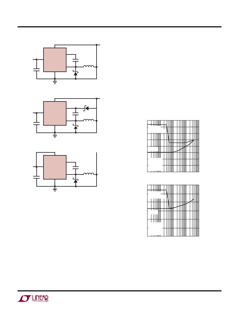
�APPLICATIONS� INFORMATION�
�BD�
�V� OUT�
�is� more� ef?cient� because� the� BOOST� pin� current� and� BD�
�pin� quiescent� current� comes� from� a� lower� voltage� source.�
�V� IN�
�4.7μF�
�V� IN�
�BOOST�
�LT1913�
�SW�
�GND�
�C3�
�You� must� also� be� sure� that� the� maximum� voltage� ratings�
�of� the� BOOST� and� BD� pins� are� not� exceeded.�
�The� minimum� operating� voltage� of� an� LT1913� application�
�is� limited� by� the� minimum� input� voltage� (3.6V)� and� by� the�
�maximum� duty� cycle� as� outlined� in� a� previous� section.� For�
�(4a)� For� V� OUT� >� 2.8V�
�proper� startup,� the� minimum� input� voltage� is� also� limited�
�by� the� boost� circuit.� If� the� input� voltage� is� ramped� slowly,�
�BD�
�BOOST�
�D2�
�V� OUT�
�or� the� LT1913� is� turned� on� with� its� RUN/SS� pin� when� the�
�output� is� already� in� regulation,� then� the� boost� capacitor�
�may� not� be� fully� charged.� Because� the� boost� capacitor� is�
�V� IN�
�V� IN�
�LT1913�
�C3�
�4.7μF�
�GND�
�SW�
�6.0�
�5.5�
�5.0�
�TO� START�
�(WORST� CASE)�
�(4b)� For� 2.5V� <� V� OUT� <� 2.8V�
�4.5�
�4.0�
�V� OUT�
�3.5�
�TO� RUN�
�V� IN�
�V� IN�
�BD�
�BOOST�
�LT1913�
�C3�
�3.0�
�2.5�
�2.0�
�V� OUT� =� 3.3V�
�T� A� =� 25°C�
�L� =� 8.2μH�
�f� =� 600kHz�
�4.7μF�
�GND�
�SW�
�1�
�10�
�100� 1000�
�LOAD� CURRENT� (mA)�
�10000�
�8.0�
�1913� FO4�
�(4c)� For� V� OUT� <� 2.5V�
�Figure� 4.� Three� Circuits� For� Generating� The� Boost� Voltage�
�more� than� 2.3V� above� the� SW� pin� for� best� ef?ciency.� For�
�outputs� of� 3V� and� above,� the� standard� circuit� (Figure� 4a)�
�7.0�
�6.0�
�5.0�
�4.0�
�TO� START�
�(WORST� CASE)�
�TO� RUN�
�is� best.� For� outputs� between� 2.8V� and� 3V,� use� a� 1μF� boost�
�capacitor.� A� 2.5V� output� presents� a� special� case� because� it�
�is� marginally� adequate� to� support� the� boosted� drive� stage�
�while� using� the� internal� boost� diode.� For� reliable� BOOST� pin�
�3.0�
�2.0�
�1�
�V� OUT� =� 5V�
�T� A� =� 25°C�
�L� =� 8.2μH�
�f� =� 600kHz�
�10�
�100� 1000�
�LOAD� CURRENT� (mA)�
�10000�
�operation� with� 2.5V� outputs� use� a� good� external� Schottky�
�diode� (such� as� the� ON� Semi� MBR0540),� and� a� 1μF� boost�
�capacitor� (see� Figure� 4b).� For� lower� output� voltages� the�
�1913� F05�
�Figure� 5.� The� Minimum� Input� Voltage� Depends� on�
�Output� Voltage,� Load� Current� and� Boost� Circuit�
�boost� diode� can� be� tied� to� the� input� (Figure� 4c),� or� to�
�another� supply� greater� than� 2.8V.� The� circuit� in� Figure� 4a�
�1913f�
�15�
�相关PDF资料 |
PDF描述 |
|---|---|
| ABB15DHRT | CONN CARD EXTEND 30POS .050" |
| ECA35DRMN-S288 | CONN EDGECARD 70POS .125 EXTEND |
| CDR125NP-330MC | POWER INDUCTOR 33UH 1.8A SMD |
| ACC18DRTH | CONN EDGECARD 36POS .100 DIP SLD |
| ECA35DRMH-S288 | CONN EDGECARD 70POS .125 EXTEND |
相关代理商/技术参数 |
参数描述 |
|---|---|
| LT1913EDD-TRPBF | 制造商:LINER 制造商全称:Linear Technology 功能描述:25V, 3.5A, 2.4MHz Step-Down Switching Regulator |
| LT1913IDD#PBF | 功能描述:IC REG BUCK ADJ 3.5A 10DFN RoHS:是 类别:集成电路 (IC) >> PMIC - 稳压器 - DC DC 开关稳压器 系列:- 标准包装:250 系列:- 类型:降压(降压) 输出类型:固定 输出数:1 输出电压:1.2V 输入电压:2.05 V ~ 6 V PWM 型:电压模式 频率 - 开关:2MHz 电流 - 输出:500mA 同步整流器:是 工作温度:-40°C ~ 85°C 安装类型:表面贴装 封装/外壳:6-UFDFN 包装:带卷 (TR) 供应商设备封装:6-SON(1.45x1) 产品目录页面:1032 (CN2011-ZH PDF) 其它名称:296-25628-2 |
| LT1913IDD#TRPBF | 功能描述:IC REG BUCK ADJ 3.5A 10DFN RoHS:是 类别:集成电路 (IC) >> PMIC - 稳压器 - DC DC 开关稳压器 系列:- 设计资源:Design Support Tool 标准包装:1 系列:- 类型:升压(升压) 输出类型:固定 输出数:1 输出电压:3V 输入电压:0.75 V ~ 2 V PWM 型:- 频率 - 开关:- 电流 - 输出:100mA 同步整流器:是 工作温度:-40°C ~ 85°C 安装类型:表面贴装 封装/外壳:SOT-23-5 细型,TSOT-23-5 包装:剪切带 (CT) 供应商设备封装:TSOT-23-5 其它名称:AS1323-BTTT-30CT |
| LT1913IDD-PBF | 制造商:LINER 制造商全称:Linear Technology 功能描述:25V, 3.5A, 2.4MHz Step-Down Switching Regulator |
| LT1913IDD-TRPBF | 制造商:LINER 制造商全称:Linear Technology 功能描述:25V, 3.5A, 2.4MHz Step-Down Switching Regulator |
发布紧急采购,3分钟左右您将得到回复。