- 您现在的位置:买卖IC网 > PDF目录2155 > LT1920IS8#TRPBF (Linear Technology)IC AMP INSTRUMENT PREC LP 8SOIC PDF资料下载
参数资料
| 型号: | LT1920IS8#TRPBF |
| 厂商: | Linear Technology |
| 文件页数: | 11/12页 |
| 文件大小: | 0K |
| 描述: | IC AMP INSTRUMENT PREC LP 8SOIC |
| 标准包装: | 2,500 |
| 放大器类型: | 仪表 |
| 电路数: | 1 |
| 转换速率: | 1.2 V/µs |
| 增益带宽积: | 1MHz |
| 电流 - 输入偏压: | 500pA |
| 电压 - 输入偏移: | 30µV |
| 电流 - 电源: | 900µA |
| 电流 - 输出 / 通道: | 27mA |
| 电压 - 电源,单路/双路(±): | 4.6 V ~ 36 V,±2.3 V ~ 18 V |
| 工作温度: | -40°C ~ 85°C |
| 安装类型: | 表面贴装 |
| 封装/外壳: | 8-SOIC(0.154",3.90mm 宽) |
| 供应商设备封装: | 8-SO |
| 包装: | 带卷 (TR) |
8
LT1920
with programmed gain. Therefore, the bandwidth does not
drop proportional to gain.
The input transistors Q1 and Q2 offer excellent matching,
which is inherent in NPN bipolar transistors, as well as
picoampere input bias current due to superbeta process-
ing. The collector currents in Q1 and Q2 are held constant
due to the feedback through the Q1-A1-R1 loop and
Q2-A2-R2 loop which in turn impresses the differential
input voltage across the external gain set resistor RG.
Since the current that flows through RG also flows through
R1 and R2, the ratios provide a gained-up differential volt-
age,G = (R1 + R2)/RG, to the unity-gain difference amplifier
A3. The common mode voltage is removed by A3, result-
ing in a single-ended output voltage referenced to the
voltage on the REF pin. The resulting gain equation is:
VOUT – VREF = G(VIN
+ – V
IN
–)
where:
G = (49.4k
/RG) + 1
solving for the gain set resistor gives:
RG = 49.4k/(G – 1)
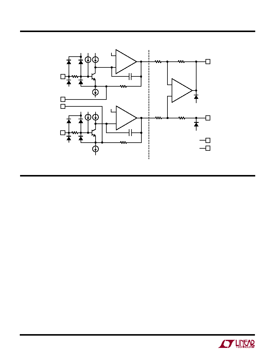
THEORY OF OPERATIO
U
The LT1920 is a modified version of the three op amp
instrumentation amplifier. Laser trimming and monolithic
construction allow tight matching and tracking of circuit
parameters over the specified temperature range. Refer to
the block diagram (Figure 1) to understand the following
circuit description. The collector currents in Q1 and Q2 are
trimmed to minimize offset voltage drift, thus assuring a
high level of performance. R1 and R2 are trimmed to an
absolute value of 24.7k to assure that the gain can be set
accurately (0.3% at G = 100) with only one external
resistor RG. The value of RG in parallel with R1 (R2)
determines the transconductance of the preamp stage. As
RG is reduced for larger programmed gains, the transcon-
ductance of the input preamp stage increases to that of the
input transistors Q1 and Q2. This increases the open-loop
gain when the programmed gain is increased, reducing
the input referred gain related errors and noise. The input
voltage noise at gains greater than 50 is determined only
by Q1 and Q2. At lower gains the noise of the difference
amplifier and preamp gain setting resistors increase the
noise. The gain bandwidth product is determined by C1,
C2 and the preamp transconductance which increases
BLOCK DIAGRAM
W
Q1
RG
2
OUTPUT
6
REF
1920 F01
5
7
–
+
A1
–
+
A3
VB
R1
24.7k
R3
400
R4
400
C1
1
RG 8
R7
10k
R8
10k
R5
10k
R6
10k
DIFFERENCE AMPLIFIER STAGE
PREAMP STAGE
+IN
–IN
3
–
+
A2
VB
R2
24.7k
C2
V +
V –
V +
V –
Q2
V –
V +
4
V –
Figure 1. Block Diagram
相关PDF资料 |
PDF描述 |
|---|---|
| LT1969CMS#TRPBF | IC OP-AMP ADJ CURRNT DUAL 10MSOP |
| LT1970IFE#TRPBF | IC OP AMP 500MA ADJ 20-TSSOP |
| LT1990AHS8#TRPBF | IC AMP DIFF +/-250V MCRPWR 8SOIC |
| LT1993CUD-10#TRPBF | IC DIFF AMP/ADC DRVR 16-QFN |
| LT1993CUD-2#PBF | IC DIFF AMP/ADC DRVR 16-QFN |
相关代理商/技术参数 |
参数描述 |
|---|---|
| LT1921G | 制造商:未知厂家 制造商全称:未知厂家 功能描述:Optoelectronic |
| LT1922G | 制造商:未知厂家 制造商全称:未知厂家 功能描述:Optoelectronic |
| LT1930 | 制造商:LINER 制造商全称:Linear Technology 功能描述:Quad DCDC Converter for Triple Outputs TFT Supply Plus LED Driver |
| LT1930/LT1930A | 制造商:LINER 制造商全称:Linear Technology 功能描述:4A, 2MHz Dual Phase Step-Up DC/DC Converter in 3mm 3mm DFN |
| LT1930A | 制造商:LINER 制造商全称:Linear Technology 功能描述:Quad DCDC Converter for Triple Outputs TFT Supply Plus LED Driver |
发布紧急采购,3分钟左右您将得到回复。