- 您现在的位置:买卖IC网 > PDF目录14118 > LT1934EDCB#TRPBF (Linear Technology)IC REG BUCK ADJ 0.3A 6DFN PDF资料下载
参数资料
| 型号: | LT1934EDCB#TRPBF |
| 厂商: | Linear Technology |
| 文件页数: | 8/20页 |
| 文件大小: | 0K |
| 描述: | IC REG BUCK ADJ 0.3A 6DFN |
| 标准包装: | 2,500 |
| 类型: | 降压(降压) |
| 输出类型: | 可调式 |
| 输出数: | 1 |
| 输出电压: | 1.25 V ~ 28 V |
| 输入电压: | 3.2 V ~ 34 V |
| PWM 型: | Burst Mode? |
| 电流 - 输出: | 300mA |
| 同步整流器: | 无 |
| 工作温度: | -40°C ~ 85°C |
| 安装类型: | 表面贴装 |
| 封装/外壳: | 6-WFDFN 裸露焊盘 |
| 包装: | 带卷 (TR) |
| 供应商设备封装: | 6-DFN-EP(2x3) |
�� �
�
�LT1934/LT1934-1�
�APPLICATIONS� INFORMATION�
�Which� One� to� Use:� LT1934� or� LT1934-1?�
�The� only� difference� between� the� LT1934� and� LT1934-1�
�is� the� peak� current� through� the� internal� switch� and� the�
�inductor.� If� your� maximum� load� current� is� less� than� 60mA,�
�use� the� LT1934-1.� If� your� maximum� load� is� higher,� use�
�the� LT1934;� it� can� supply� up� to� ~300mA.�
�While� the� LT1934-1� can’t� deliver� as� much� output� current,�
�it� has� other� advantages.� The� lower� peak� switch� current�
�allows� the� use� of� smaller� components� (input� capacitor,�
�inductor� and� output� capacitor).� The� ripple� current� at� the�
�input� of� the� LT1934-1� circuit� will� be� smaller� and� may� be�
�an� important� consideration� if� the� input� supply� is� current�
�limited� or� has� high� impedance.� The� LT1934-1’s� current�
�draw� during� faults� (output� overload� or� short)� and� start-�
�up� is� lower.�
�The� maximum� load� current� that� the� LT1934� or� LT1934-1�
�can� deliver� depends� on� the� value� of� the� inductor� used.�
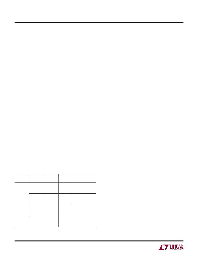
�Table� 1� lists� inductor� value,� minimum� output� capacitor�
�and� maximum� load� for� 3.3V� and� 5V� circuits.� Increasing�
�the� value� of� the� capacitor� will� lower� the� output� voltage�
�ripple.� Component� selection� is� covered� in� more� detail� in�
�the� following� sections.�
�Minimum� Input� Voltage�
�The� minimum� input� voltage� required� to� generate� a� par-�
�ticular� output� voltage� is� determined� by� either� the� LT1934’s�
�undervoltage� lockout� of� ~3V� or� by� its� maximum� duty� cycle.�
�The� duty� cycle� is� the� fraction� of� time� that� the� internal�
�switch� is� on� and� is� determined� by� the� input� and� output�
�voltages:�
�DC� =� (V� OUT� +� V� D� )/(V� IN� –� V� SW� +� V� D� )�
�where� V� D� is� the� forward� voltage� drop� of� the� catch� diode�
�(~0.4V)� and� V� SW� is� the� voltage� drop� of� the� internal� switch�
�(~0.3V� at� maximum� load� for� the� LT1934,� ~0.1V� for� the�
�LT1934-1).� This� leads� to� a� minimum� input� voltage� of:�
�V� IN(MIN)� =� (V� OUT� +� V� D� )/DC� MAX� –� V� D� +� V� SW�
�with� DC� MAX� =� 0.85.�
�Inductor� Selection�
�A� good� ?rst� choice� for� the� inductor� value� is:�
�L� =� 2.5� ?� (V� OUT� +� V� D� )� ?� 1.8μs/I� LIM�
�where� I� LIM� is� the� switch� current� limit� (400mA� for� the�
�LT1934� and� 120mA� for� the� LT1934-1).� This� choice� provides�
�a� worst-case� maximum� load� current� of� 250mA� (60mA� for�
�the� LT1934-1).� The� inductor’s� RMS� current� rating� must�
�be� greater� than� the� load� current� and� its� saturation� current�
�should� be� greater� than� I� LIM� .� To� keep� ef?ciency� high,� the�
�series� resistance� (DCR)� should� be� less� than� 0.3Ω� (1Ω�
�for� the� LT1934-1).� Table� 2� lists� several� vendors� and� types�
�that� are� suitable.�
�This� simple� rule� may� not� provide� the� optimum� value� for�
�your� application.� If� the� load� current� is� less,� then� you� can�
�relax� the� value� of� the� inductor� and� operate� with� higher�
�Table� 1�
�PART�
�LT1934�
�LT1934-1�
�V� OUT�
�3.3V�
�5V�
�3.3V�
�5V�
�L�
�100μH�
�47μH�
�33μH�
�150μH�
�68μH�
�47μH�
�150μH�
�100μH�
�68μH�
�220μH�
�150μH�
�100μH�
�MINIMUM�
�C� OUT�
�100μH�
�47μH�
�33μH�
�47μH�
�33μH�
�22μH�
�15μH�
�10μH�
�10μH�
�10μH�
�4.7μH�
�4.7μH�
�MAXIMUM�
�LOAD�
�300mA�
�250mA�
�200mA�
�300mA�
�250mA�
�200mA�
�60mA�
�45mA�
�20mA�
�60mA�
�45mA�
�20mA�
�ripple� current.� This� allows� you� to� use� a� physically� smaller�
�inductor,� or� one� with� a� lower� DCR� resulting� in� higher�
�ef?ciency.� The� following� provides� more� details� to� guide�
�inductor� selection.� First,� the� value� must� be� chosen� so� that�
�the� LT1934� can� supply� the� maximum� load� current� drawn�
�from� the� output.� Second,� the� inductor� must� be� rated� ap-�
�propriately� so� that� the� LT1934� will� function� reliably� and�
�the� inductor� itself� will� not� be� overly� stressed.�
�Detailed� Inductor� Selection� and�
�Maximum� Load� Current�
�The� square� wave� that� the� LT1934� produces� at� its� switch�
�pin� results� in� a� triangle� wave� of� current� in� the� inductor.� The�
�LT1934� limits� the� peak� inductor� current� to� I� LIM� .� Because�
�1934fe�
�8�
�相关PDF资料 |
PDF描述 |
|---|---|
| EBC43DRTN-S734 | CONN EDGECARD 86POS DIP .100 SLD |
| LT1934ES6#TRPBF | IC REG BUCK ADJ 0.3A SOT23-6 |
| LT1934ES6#TR | IC REG BUCK ADJ 0.3A SOT23-6 |
| EBC43DRTH-S734 | CONN EDGECARD 86POS DIP .100 SLD |
| LT1934ES6-1#TRPBF | IC REG BUCK ADJ 60MA SOT23-6 |
相关代理商/技术参数 |
参数描述 |
|---|---|
| LT1934ES6 | 制造商:Linear Technology 功能描述:Conv DC-DC Single Step Down 3.2V to 34V 6-Pin TSOT-23 |
| LT1934ES6#PBF | 制造商:Linear Technology 功能描述:Conv DC-DC Single Step Down 3.2V to 34V 6-Pin TSOT-23 制造商:Linear Technology 功能描述:IC DC-DC CONV 6-SOT-23 |
| LT1934ES6#TR | 功能描述:IC REG BUCK ADJ 0.3A SOT23-6 RoHS:否 类别:集成电路 (IC) >> PMIC - 稳压器 - DC DC 开关稳压器 系列:- 标准包装:2,500 系列:- 类型:升压(升压) 输出类型:可调式 输出数:1 输出电压:1.24 V ~ 30 V 输入电压:1.5 V ~ 12 V PWM 型:电流模式,混合 频率 - 开关:600kHz 电流 - 输出:500mA 同步整流器:无 工作温度:-40°C ~ 85°C 安装类型:表面贴装 封装/外壳:8-SOIC(0.154",3.90mm 宽) 包装:带卷 (TR) 供应商设备封装:8-SOIC |
| LT1934ES6#TRM | 功能描述:IC REG BUCK ADJ 0.3A SOT23-6 RoHS:否 类别:集成电路 (IC) >> PMIC - 稳压器 - DC DC 开关稳压器 系列:- 标准包装:2,500 系列:- 类型:升压(升压) 输出类型:可调式 输出数:1 输出电压:1.24 V ~ 30 V 输入电压:1.5 V ~ 12 V PWM 型:电流模式,混合 频率 - 开关:600kHz 电流 - 输出:500mA 同步整流器:无 工作温度:-40°C ~ 85°C 安装类型:表面贴装 封装/外壳:8-SOIC(0.154",3.90mm 宽) 包装:带卷 (TR) 供应商设备封装:8-SOIC |
| LT1934ES6#TRMPBF | 功能描述:IC REG BUCK ADJ 0.3A SOT23-6 RoHS:是 类别:集成电路 (IC) >> PMIC - 稳压器 - DC DC 开关稳压器 系列:- 标准包装:250 系列:- 类型:降压(降压) 输出类型:固定 输出数:1 输出电压:1.2V 输入电压:2.05 V ~ 6 V PWM 型:电压模式 频率 - 开关:2MHz 电流 - 输出:500mA 同步整流器:是 工作温度:-40°C ~ 85°C 安装类型:表面贴装 封装/外壳:6-UFDFN 包装:带卷 (TR) 供应商设备封装:6-SON(1.45x1) 产品目录页面:1032 (CN2011-ZH PDF) 其它名称:296-25628-2 |
发布紧急采购,3分钟左右您将得到回复。