参数资料
| 型号: | LT1934IDCB-1#TRPBF |
| 厂商: | Linear Technology |
| 文件页数: | 11/20页 |
| 文件大小: | 0K |
| 描述: | IC REG BUCK ADJ 60MA 6DFN |
| 标准包装: | 2,500 |
| 类型: | 降压(降压) |
| 输出类型: | 可调式 |
| 输出数: | 1 |
| 输出电压: | 1.25 V ~ 28 V |
| 输入电压: | 3.2 V ~ 34 V |
| PWM 型: | Burst Mode? |
| 电流 - 输出: | 60mA |
| 同步整流器: | 无 |
| 工作温度: | -40°C ~ 125°C |
| 安装类型: | 表面贴装 |
| 封装/外壳: | 6-WFDFN 裸露焊盘 |
| 包装: | 带卷 (TR) |
| 供应商设备封装: | 6-DFN-EP(2x3) |
�� �
�
�LT1934/LT1934-1�
�APPLICATIONS� INFORMATION�
�when� used� with� ceramic� capacitors� will� be� lower� and� may�
�be� acceptable.�
�D2�
�A� ?nal� precaution� regarding� ceramic� capacitors� concerns�
�the� maximum� input� voltage� rating� of� the� LT1934.� A� ceramic�
�V� IN�
�V� IN�
�BOOST�
�LT1934�
�SW�
�C3�
�V� OUT�
�input� capacitor� combined� with� trace� or� cable� inductance�
�forms� a� high� quality� (under� damped)� tank� circuit.� If� the�
�GND�
�LT1934� circuit� is� plugged� into� a� live� supply,� the� input� volt-�
�age� can� ring� to� twice� its� nominal� value,� possibly� exceeding�
�the� LT1934’s� rating.� This� situation� is� easily� avoided;� see�
�the� Hot� Plugging� Safely� section.�
�V� BOOST� –� V� SW�
�MAX� V� BOOST�
�D2�
�V� OUT�
�V� IN� +� V� OUT�
�(2a)�
�Catch� Diode�
�BOOST�
�LT1934�
�C3�
�A� 0.5A� Schottky� diode� is� recommended� for� the� catch�
�diode,� D1.� The� diode� must� have� a� reverse� voltage� rating�
�equal� to� or� greater� than� the� maximum� input� voltage.� The�
�ON� Semiconductor� MBR0540� is� a� good� choice;� it� is� rated�
�for� 0.5A� forward� current� and� a� maximum� reverse� voltage�
�V� IN�
�V� IN�
�GND�
�V� BOOST� –� V� SW� V� IN�
�MAX� V� BOOST�
�2V� IN�
�SW�
�V� OUT�
�1934� F02�
�of� 40V.�
�Schottky� diodes� with� lower� reverse� voltage� ratings� usu-�
�ally� have� a� lower� forward� drop� and� may� result� in� higher�
�ef?ciency� with� moderate� to� high� load� currents.� However,�
�these� diodes� also� have� higher� leakage� currents.� This� leakage�
�current� mimics� a� load� current� at� the� output� and� can� raise�
�the� quiescent� current� of� the� LT1934� circuit,� especially� at�
�elevated� temperatures.�
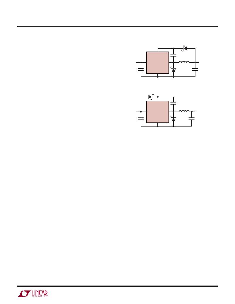
�BOOST� Pin� Considerations�
�Capacitor� C3� and� diode� D2� are� used� to� generate� a� boost�
�voltage� that� is� higher� than� the� input� voltage.� In� most� cases�
�a� 0.1μF� capacitor� and� fast� switching� diode� (such� as� the�
�1N4148� or� 1N914)� will� work� well.� Figure� 2� shows� two�
�ways� to� arrange� the� boost� circuit.� The� BOOST� pin� must�
�be� more� than� 2.5V� above� the� SW� pin� for� best� ef?ciency.�
�For� outputs� of� 3.3V� and� above,� the� standard� circuit� (Fig-�
�ure� 2a)� is� best.� For� outputs� between� 2.8V� and� 3V,� use� a�
�0.22μF� capacitor� and� a� small� Schottky� diode� (such� as� the�
�BAT-54).� For� lower� output� voltages� the� boost� diode� can� be�
�tied� to� the� input� (Figure� 2b).� The� circuit� in� Figure� 2a� is� more�
�ef?cient� because� the� BOOST� pin� current� comes� from� a� lower�
�voltage� source.� You� must� also� be� sure� that� the� maximum�
�voltage� rating� of� the� BOOST� pin� is� not� exceeded.�
�The� minimum� operating� voltage� of� an� LT1934� applica-�
�tion� is� limited� by� the� undervoltage� lockout� (~3V)� and� by�
�(2b)�
�Figure� 2.� Two� Circuits� for� Generating� the� Boost� Voltage�
�the� maximum� duty� cycle� as� outlined� above.� For� proper�
�start-up,� the� minimum� input� voltage� is� also� limited� by� the�
�boost� circuit.� If� the� input� voltage� is� ramped� slowly,� or� the�
�LT1934� is� turned� on� with� its� SHDN� pin� when� the� output�
�is� already� in� regulation,� then� the� boost� capacitor� may� not�
�be� fully� charged.� Because� the� boost� capacitor� is� charged�
�with� the� energy� stored� in� the� inductor,� the� circuit� will� rely�
�on� some� minimum� load� current� to� get� the� boost� circuit�
�running� properly.� This� minimum� load� will� depend� on� input�
�and� output� voltages,� and� on� the� arrangement� of� the� boost�
�circuit.� The� minimum� load� generally� goes� to� zero� once� the�
�circuit� has� started.� Figure� 3� shows� a� plot� of� minimum� load�
�to� start� and� to� run� as� a� function� of� input� voltage.� In� many�
�cases� the� discharged� output� capacitor� will� present� a� load�
�to� the� switcher� which� will� allow� it� to� start.� The� plots� show�
�the� worst-case� situation� where� V� IN� is� ramping� very� slowly.�
�Use� a� Schottky� diode� (such� as� the� BAT-54)� for� the� lowest�
�start-up� voltage.�
�At� light� loads,� the� inductor� current� becomes� discontinu-�
�ous� and� the� effective� duty� cycle� can� be� very� high.� This�
�reduces� the� minimum� input� voltage� to� approximately�
�300mV� above� V� OUT� .� At� higher� load� currents,� the� inductor�
�current� is� continuous� and� the� duty� cycle� is� limited� by� the�
�1934fe�
�11�
�相关PDF资料 |
PDF描述 |
|---|---|
| LT1935ES5#TRM | IC REG BST FLYBK SEPIC TSOT23-5 |
| LT1936HMS8E#TRPBF | IC REG BUCK ADJ 1.4A 8MSOP |
| LT1938IDD#TRPBF | IC REG BUCK ADJ 2.2A 10DFN |
| LT1940EFE#TRPBF | IC REG BUCK ADJ 1.4A DL 16TSSOP |
| LT1941EFE#TRPBF | IC REG MULTI CONFIG TRPL 28TSSOP |
相关代理商/技术参数 |
参数描述 |
|---|---|
| LT1934IS6 | 制造商:LINER 制造商全称:Linear Technology 功能描述:Micropower Step-Down Switching Regulators in ThinSOT |
| LT1934IS6#PBF | 制造商:Linear Technology 功能描述:Conv DC-DC Single Step Down 3.2V to 34V 6-Pin TSOT-23 制造商:Linear Technology 功能描述:SP-SWREG/Monolithic, Cut Tape 300mA (Iout), Micropower Step-Down |
| LT1934IS6#TR | 功能描述:IC REG BUCK ADJ 0.3A SOT23-6 RoHS:否 类别:集成电路 (IC) >> PMIC - 稳压器 - DC DC 开关稳压器 系列:- 标准包装:2,500 系列:- 类型:升压(升压) 输出类型:可调式 输出数:1 输出电压:1.24 V ~ 30 V 输入电压:1.5 V ~ 12 V PWM 型:电流模式,混合 频率 - 开关:600kHz 电流 - 输出:500mA 同步整流器:无 工作温度:-40°C ~ 85°C 安装类型:表面贴装 封装/外壳:8-SOIC(0.154",3.90mm 宽) 包装:带卷 (TR) 供应商设备封装:8-SOIC |
| LT1934IS6#TRM | 功能描述:IC REG BUCK ADJ 0.3A SOT23-6 RoHS:否 类别:集成电路 (IC) >> PMIC - 稳压器 - DC DC 开关稳压器 系列:- 标准包装:2,500 系列:- 类型:降压(降压) 输出类型:固定 输出数:1 输出电压:1.2V,1.5V,1.8V,2.5V 输入电压:2.7 V ~ 20 V PWM 型:- 频率 - 开关:- 电流 - 输出:50mA 同步整流器:是 工作温度:-40°C ~ 125°C 安装类型:表面贴装 封装/外壳:10-TFSOP,10-MSOP(0.118",3.00mm 宽)裸露焊盘 包装:带卷 (TR) 供应商设备封装:10-MSOP 裸露焊盘 |
| LT1934IS6#TRMPBF | 功能描述:IC REG BUCK ADJ 0.3A SOT23-6 RoHS:是 类别:集成电路 (IC) >> PMIC - 稳压器 - DC DC 开关稳压器 系列:- 标准包装:2,500 系列:- 类型:升压(升压) 输出类型:可调式 输出数:1 输出电压:1.24 V ~ 30 V 输入电压:1.5 V ~ 12 V PWM 型:电流模式,混合 频率 - 开关:600kHz 电流 - 输出:500mA 同步整流器:无 工作温度:-40°C ~ 85°C 安装类型:表面贴装 封装/外壳:8-SOIC(0.154",3.90mm 宽) 包装:带卷 (TR) 供应商设备封装:8-SOIC |
发布紧急采购,3分钟左右您将得到回复。