- 您现在的位置:买卖IC网 > PDF目录44983 > LT1934IS6-1#PBF (LINEAR TECHNOLOGY CORP) 0.16 A SWITCHING REGULATOR, PDSO6 PDF资料下载
参数资料
| 型号: | LT1934IS6-1#PBF |
| 厂商: | LINEAR TECHNOLOGY CORP |
| 元件分类: | 稳压器 |
| 英文描述: | 0.16 A SWITCHING REGULATOR, PDSO6 |
| 封装: | 1 MM HEIGHT, LEAD FREE, PLASTIC, MO-193, TSOT-6 |
| 文件页数: | 3/20页 |
| 文件大小: | 234K |
| 代理商: | LT1934IS6-1#PBF |
LT1934/LT1934-1
11
1934fe
APPLICATIONS INFORMATION
when used with ceramic capacitors will be lower and may
be acceptable.
A nal precaution regarding ceramic capacitors concerns
the maximum input voltage rating of the LT1934. A ceramic
input capacitor combined with trace or cable inductance
forms a high quality (under damped) tank circuit. If the
LT1934 circuit is plugged into a live supply, the input volt-
age can ring to twice its nominal value, possibly exceeding
the LT1934’s rating. This situation is easily avoided; see
the Hot Plugging Safely section.
Catch Diode
A 0.5A Schottky diode is recommended for the catch
diode, D1. The diode must have a reverse voltage rating
equal to or greater than the maximum input voltage. The
ON Semiconductor MBR0540 is a good choice; it is rated
for 0.5A forward current and a maximum reverse voltage
of 40V.
Schottky diodes with lower reverse voltage ratings usu-
ally have a lower forward drop and may result in higher
efciency with moderate to high load currents. However,
these diodes also have higher leakage currents. This leakage
current mimics a load current at the output and can raise
the quiescent current of the LT1934 circuit, especially at
elevated temperatures.
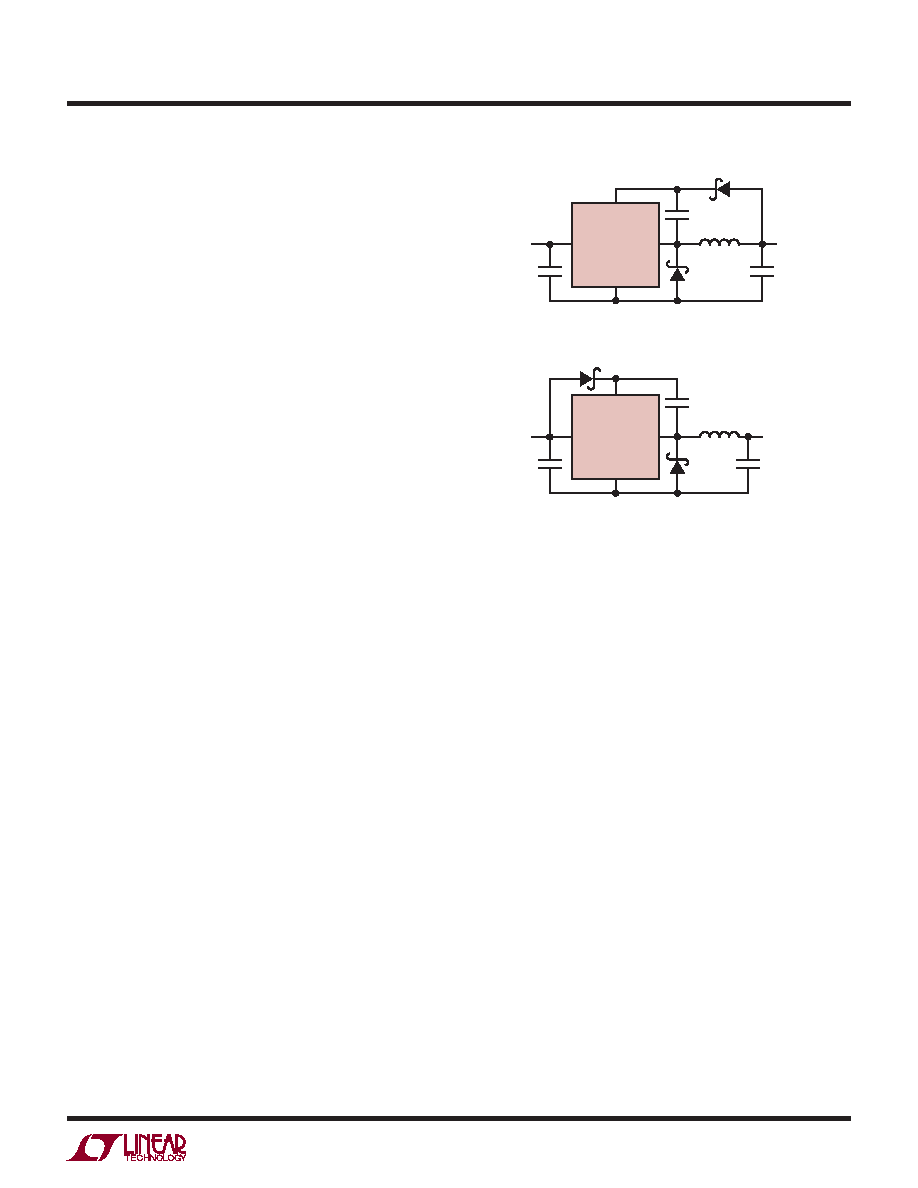
BOOST Pin Considerations
Capacitor C3 and diode D2 are used to generate a boost
voltage that is higher than the input voltage. In most cases
a 0.1μF capacitor and fast switching diode (such as the
1N4148 or 1N914) will work well. Figure 2 shows two
ways to arrange the boost circuit. The BOOST pin must
be more than 2.5V above the SW pin for best efciency.
For outputs of 3.3V and above, the standard circuit (Fig-
ure 2a) is best. For outputs between 2.8V and 3V, use a
0.22μF capacitor and a small Schottky diode (such as the
BAT-54). For lower output voltages the boost diode can be
tied to the input (Figure 2b). The circuit in Figure 2a is more
efcient because the BOOST pin current comes from a lower
voltage source. You must also be sure that the maximum
voltage rating of the BOOST pin is not exceeded.
The minimum operating voltage of an LT1934 applica-
tion is limited by the undervoltage lockout (~3V) and by
the maximum duty cycle as outlined above. For proper
start-up, the minimum input voltage is also limited by the
boost circuit. If the input voltage is ramped slowly, or the
LT1934 is turned on with its SHDN pin when the output
is already in regulation, then the boost capacitor may not
be fully charged. Because the boost capacitor is charged
with the energy stored in the inductor, the circuit will rely
on some minimum load current to get the boost circuit
running properly. This minimum load will depend on input
and output voltages, and on the arrangement of the boost
circuit. The minimum load generally goes to zero once the
circuit has started. Figure 3 shows a plot of minimum load
to start and to run as a function of input voltage. In many
cases the discharged output capacitor will present a load
to the switcher which will allow it to start. The plots show
the worst-case situation where VIN is ramping very slowly.
Use a Schottky diode (such as the BAT-54) for the lowest
start-up voltage.
At light loads, the inductor current becomes discontinu-
ous and the effective duty cycle can be very high. This
reduces the minimum input voltage to approximately
300mV above VOUT. At higher load currents, the inductor
current is continuous and the duty cycle is limited by the
VIN
BOOST
GND
SW
VIN
LT1934
(2a)
D2
VOUT
C3
VBOOST – VSW VOUT
MAX VBOOST VIN + VOUT
VIN
BOOST
GND
SW
VIN
LT1934
(2b)
D2
1934 F02
VOUT
C3
VBOOST – VSW VIN
MAX VBOOST 2VIN
Figure 2. Two Circuits for Generating the Boost Voltage
相关PDF资料 |
PDF描述 |
|---|---|
| LT1938IDD#PBF | 4 A SWITCHING REGULATOR, 3300 kHz SWITCHING FREQ-MAX, PDSO10 |
| LT1956-5EGN | 3 A SWITCHING REGULATOR, 570 kHz SWITCHING FREQ-MAX, PDSO16 |
| LT1956-5IGN | 3 A SWITCHING REGULATOR, 570 kHz SWITCHING FREQ-MAX, PDSO16 |
| LT1961IMS8E#TR | 3 A SWITCHING REGULATOR, 1500 kHz SWITCHING FREQ-MAX, PDSO8 |
| LT3092ITS8#PBF | SPECIALTY ANALOG CIRCUIT, PDSO8 |
相关代理商/技术参数 |
参数描述 |
|---|---|
| LT1934IS6TRMPBF | 制造商:Linear Technology 功能描述:DC-DC Converter Step-Down 34V TSOT23-6 |
| LT1935 | 制造商:LINER 制造商全称:Linear Technology 功能描述:1.2MHz Boost DC/DC Converter in ThinSOT with 2A Switch |
| LT1935ES5 | 制造商:Linear Technology 功能描述:Conv DC-DC Single Step Up 2.3V to 16V 5-Pin TSOT-23 |
| LT1935ES5#PBF | 制造商:Linear Technology 功能描述:Conv DC-DC Single Step Up 2.3V to 16V 5-Pin TSOT-23 制造商:Linear Technology 功能描述:DC-DC CONVERTER BOOST 1.2MHZ 制造商:Linear Technology 功能描述:DC-DC CONVERTER, BOOST, 1.2MHZ, SOT-23-5; Primary Input Voltage:16V; No. of Outputs:1; Output Current:3.2A; No. of Pins:5; Operating Temperature Min:-40C; Operating Temperature Max:85C; Operating Temperature Range:-40C to +85C ;RoHS Compliant: Yes 制造商:Linear Technology 功能描述:DC-DC CONVERTER, BOOST, 1.2MHZ, SOT-23-5; Primary Input Voltage:16V; No. of Outputs:1; Output Voltage:38V; Output Current:3.2A; No. of Pins:5; Operating Temperature Min:-40C; Operating Temperature Max:85C; Package / Case:5-TSOT-23 ;RoHS Compliant: Yes |
| LT1935ES5#TR | 功能描述:IC REG BST FLYBK SEPIC TSOT23-5 RoHS:否 类别:集成电路 (IC) >> PMIC - 稳压器 - DC DC 开关稳压器 系列:- 标准包装:2,500 系列:- 类型:升压(升压) 输出类型:可调式 输出数:1 输出电压:1.24 V ~ 30 V 输入电压:1.5 V ~ 12 V PWM 型:电流模式,混合 频率 - 开关:600kHz 电流 - 输出:500mA 同步整流器:无 工作温度:-40°C ~ 85°C 安装类型:表面贴装 封装/外壳:8-SOIC(0.154",3.90mm 宽) 包装:带卷 (TR) 供应商设备封装:8-SOIC |
发布紧急采购,3分钟左右您将得到回复。