- 您现在的位置:买卖IC网 > PDF目录44983 > LT1938IDD#PBF (LINEAR TECHNOLOGY CORP) 4 A SWITCHING REGULATOR, 3300 kHz SWITCHING FREQ-MAX, PDSO10 PDF资料下载
参数资料
| 型号: | LT1938IDD#PBF |
| 厂商: | LINEAR TECHNOLOGY CORP |
| 元件分类: | 稳压器 |
| 英文描述: | 4 A SWITCHING REGULATOR, 3300 kHz SWITCHING FREQ-MAX, PDSO10 |
| 封装: | 3 X 3 MM, LEAD FREE, PLASTIC, MO-229WEED-2, DFN-10 |
| 文件页数: | 7/24页 |
| 文件大小: | 260K |
| 代理商: | LT1938IDD#PBF |
LT1938
15
1938fa
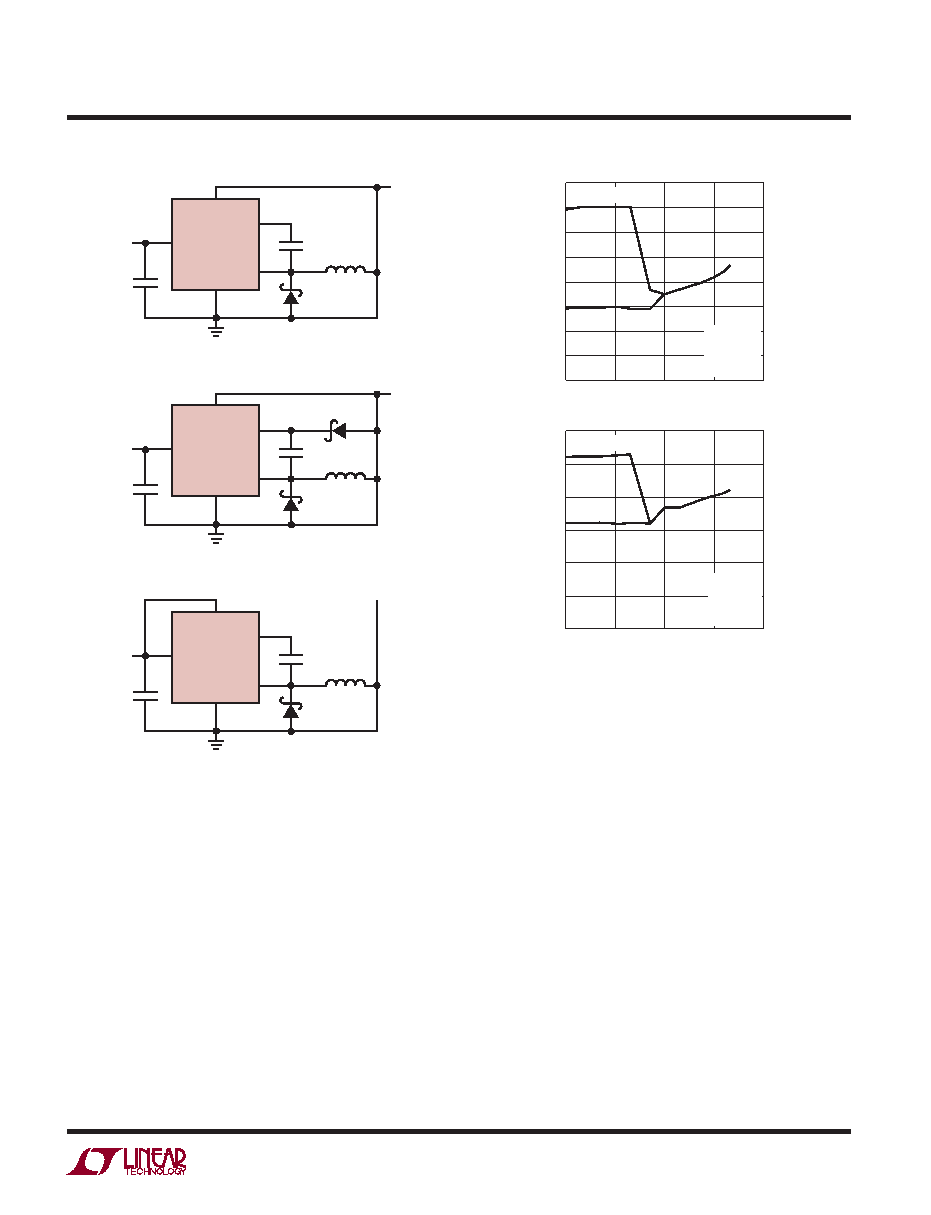
proper start-up, the minimum input voltage is also limited
by the boost circuit. If the input voltage is ramped slowly,
or the LT1938 is turned on with its RUN/SS pin when the
output is already in regulation, then the boost capacitor
may not be fully charged. Because the boost capacitor is
charged with the energy stored in the inductor, the circuit
will rely on some minimum load current to get the boost
circuit running properly. This minimum load will depend
on input and output voltages, and on the arrangement of
the boost circuit. The minimum load generally goes to
zero once the circuit has started. Figure 5 shows a plot
of minimum load to start and to run as a function of input
voltage. In many cases the discharged output capacitor
will present a load to the switcher and the minimum input
to start will be the same as the minimum input to run.
This occurs, for example, if RUN/SS is asserted after VIN
is applied. The plots show the worst-case situation where
VIN is ramping very slowly. For lower start-up voltage, the
boost diode can be tied to VIN; however, this restricts the
input range to one-half of the absolute maximum rating
of the BOOST pin.
At light loads, the inductor current becomes discontinu-
ous and the effective duty cycle can be very high. This
reduces the minimum input voltage to approximately
300mV above VOUT. At higher load currents, the inductor
current is continuous and the duty cycle is limited by the
maximum duty cycle of the LT1938, requiring a higher
input voltage to maintain regulation.
Figure 4. Three Circuits For Generating The Boost Voltage
Figure 5. The Minimum Input Voltage Depends on
Output Voltage, Load Current and Boost Circuit
APPLICATIONS INFORMATION
VIN
BOOST
SW
BD
VIN
VOUT
4.7F
C3
GND
LT1938
VIN
BOOST
SW
BD
VIN
VOUT
4.7F
C3
D2
GND
LT1938
VIN
BOOST
SW
BD
VIN
VOUT
4.7F
C3
GND
LT1938
1938 F04
(4a) For VOUT > 2.8V
(4b) For 2.5V < VOUT < 2.8V
(4c) For VOUT < 2.5V
1938 F05
LOAD CURRENT (A)
0.001
INPUT
VOL
TAGE
(V)
4.0
4.5
5.0
10
3.5
3.0
2.0
0.01
0.1
1
2.5
6.0
5.5
TO START
TO RUN
VOUT = 3.3V
TA = 25°C
L = 4.7H
f = 800kHz
LOAD CURRENT (A)
0.001
INPUT
VOL
TAGE
(V)
5.0
6.0
7.0
10
4.0
2.0
0.01
0.1
1
3.0
8.0
TO START
TO RUN
VOUT = 5V
TA = 25°C
L = 4.7H
f = 800kHz
相关PDF资料 |
PDF描述 |
|---|---|
| LT1956-5EGN | 3 A SWITCHING REGULATOR, 570 kHz SWITCHING FREQ-MAX, PDSO16 |
| LT1956-5IGN | 3 A SWITCHING REGULATOR, 570 kHz SWITCHING FREQ-MAX, PDSO16 |
| LT1961IMS8E#TR | 3 A SWITCHING REGULATOR, 1500 kHz SWITCHING FREQ-MAX, PDSO8 |
| LT3092ITS8#PBF | SPECIALTY ANALOG CIRCUIT, PDSO8 |
| LT3092ETS8#TRPBF | SPECIALTY ANALOG CIRCUIT, PDSO8 |
相关代理商/技术参数 |
参数描述 |
|---|---|
| LT1939 | 制造商:LINER 制造商全称:Linear Technology 功能描述:Monolithic 2A Step-Down Regulator Plus Linear Regulator/Controller |
| LT1939EDD#PBF | 功能描述:IC REG DL BUCK/LINEAR 12DFN RoHS:是 类别:集成电路 (IC) >> PMIC - 稳压器 - 线性 + 切换式 系列:- 标准包装:2,500 系列:- 拓扑:降压(降压)同步(3),线性(LDO)(2) 功能:任何功能 输出数:5 频率 - 开关:300kHz 电压/电流 - 输出 1:控制器 电压/电流 - 输出 2:控制器 电压/电流 - 输出 3:控制器 带 LED 驱动器:无 带监控器:无 带序列发生器:是 电源电压:5.6 V ~ 24 V 工作温度:-40°C ~ 85°C 安装类型:* 封装/外壳:* 供应商设备封装:* 包装:* |
| LT1939EDD#TRPBF | 功能描述:IC REG DL BUCK/LINEAR 12DFN RoHS:是 类别:集成电路 (IC) >> PMIC - 稳压器 - 线性 + 切换式 系列:- 标准包装:2,500 系列:- 拓扑:降压(降压)同步(3),线性(LDO)(2) 功能:任何功能 输出数:5 频率 - 开关:300kHz 电压/电流 - 输出 1:控制器 电压/电流 - 输出 2:控制器 电压/电流 - 输出 3:控制器 带 LED 驱动器:无 带监控器:无 带序列发生器:是 电源电压:5.6 V ~ 24 V 工作温度:-40°C ~ 85°C 安装类型:* 封装/外壳:* 供应商设备封装:* 包装:* |
| LT1939EDD-PBF | 制造商:LINER 制造商全称:Linear Technology 功能描述:Monolithic 2A Step-Down Regulator Plus Linear Regulator/Controller |
| LT1939EDD-TRPBF | 制造商:LINER 制造商全称:Linear Technology 功能描述:Monolithic 2A Step-Down Regulator Plus Linear Regulator/Controller |
发布紧急采购,3分钟左右您将得到回复。