- 您现在的位置:买卖IC网 > PDF目录53672 > LT1945IMS#PBF (LINEAR TECHNOLOGY CORP) DUAL SWITCHING CONTROLLER, PDSO8 PDF资料下载
参数资料
| 型号: | LT1945IMS#PBF |
| 厂商: | LINEAR TECHNOLOGY CORP |
| 元件分类: | 稳压器 |
| 英文描述: | DUAL SWITCHING CONTROLLER, PDSO8 |
| 封装: | LEAD FREE, PLASTIC, MSOP-8 |
| 文件页数: | 4/8页 |
| 文件大小: | 121K |
| 代理商: | LT1945IMS#PBF |
LT1945
4
1945fa
PIN FUNCTIONS
NFB1 (Pin 1): Feedback Pin for Switcher 1. Set the output
voltage by selecting values for R1 and R2.
SHDN1 (Pin 2): Shutdown Pin for Switcher 1. Tie this
pin to 0.9V or higher to enable device. Tie below 0.25V
to turn it off.
GND (Pin 3): Ground. Tie this pin directly to the local
ground plane.
SHDN2 (Pin 4): Shutdown Pin for Switcher 2. Tie this
pin to 0.9V or higher to enable device. Tie below 0.25V
to turn it off.
FB2 (Pin 5): Feedback Pin for Switcher 2. Set the output
voltage by selecting values for R1B and R2B.
SW2 (Pin 6): Switch Pin for Switcher 2. This is the
collector of the internal NPN power switch. Minimize the
metal trace area connected to the pin to minimize EMI.
PGND (Pins 7, 9): Power Ground. Tie these pins directly
to the local ground plane. Both pins must be tied.
VIN (Pin 8): Input Supply Pin. Bypass this pin with a
capacitor as close to the device as possible.
SW1 (Pin 10): Switch Pin for Switcher 1. This is the
collector of the internal NPN power switch. Minimize the
metal trace area connected to the pin to minimize EMI.
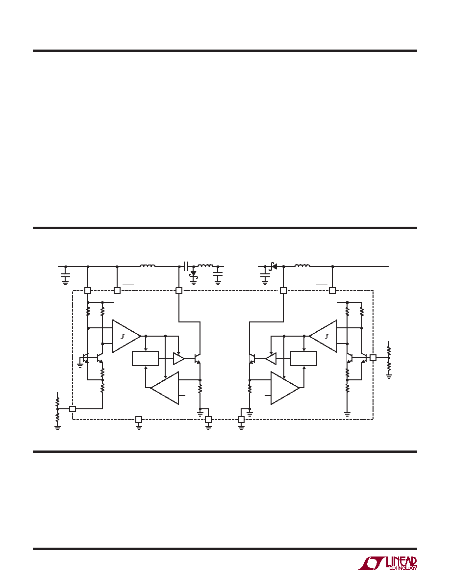
BLOCK DIAGRAM
–
+
–
+
8
400ns
ONE-SHOT
DRIVER
RESET
ENABLE
42mV
0.12Ω
A2
A1
Q3
9
3
R4
280k
R3
60k
R6
80k
R5
80k
Q2
X10
Q1
1
VIN
NFB1
2
SHDN1
10
SW1
PGND
GND
1945 BD
L1
C3
C2
VOUT1
VIN
D1
R2
(EXTERNAL)
R1
(EXTERNAL)
VOUT1
C1
–
+
–
+
400ns
ONE-SHOT
ENABLE
42mV
0.12Ω
A2B
A1B
Q3B
7
R4B
140k
R3B
30k
R6B
40k
R5B
40k
Q2B
X10
Q1B
5
VIN
FB2
4
SHDN2
6
SW2
PGND
L3
L2
C4
VOUT2
VIN
D2
R2B
(EXTERNAL)
R1B
(EXTERNAL)
VOUT2
SWITCHER 1
SWITCHER 2
DRIVER
Figure 1. LT1945 Block Diagram
OPERATION
The LT1945 uses a constant off-time control scheme
to provide high efciencies over a wide range of output
current. Operation can be best understood by referring
to the block diagram in Figure 1. Q1 and Q2 along with
R3 and R4 form a bandgap reference used to regulate
the output voltage. When the voltage at the NFB1 pin is
slightly below –1.23V, comparator A1 disables most of
the internal circuitry. Output current is then provided by
capacitor C2, which slowly discharges until the voltage
at the NFB1 pin goes above the hysteresis point of A1
(typical hysteresis at the NFB1 pin is 8mV). A1 then enables
the internal circuitry, turns on power switch Q3, and the
相关PDF资料 |
PDF描述 |
|---|---|
| LT1945IMS#TR | DUAL SWITCHING CONTROLLER, PDSO8 |
| LT1948EMS8#TR | 1.5 A SWITCHING REGULATOR, 3600 kHz SWITCHING FREQ-MAX, PDSO8 |
| LT253A | SPECIALTY ANALOG CIRCUIT, PDSO4 |
| LT3464DICE | 0.14 A SWITCHING REGULATOR, UUC8 |
| LTC1174IS8-3.3#TRPBF | SWITCHING REGULATOR, PDSO8 |
相关代理商/技术参数 |
参数描述 |
|---|---|
| LT1946 | 制造商:LINER 制造商全称:Linear Technology 功能描述:1.2MHz Boost DC/DC Converter with 1.5A Switch and Soft-Start |
| LT1946/LT1946A | 制造商:LINER 制造商全称:Linear Technology 功能描述:4A, 2MHz Dual Phase Step-Up DC/DC Converter in 3mm 3mm DFN |
| LT1946A | 制造商:LINER 制造商全称:Linear Technology 功能描述:1.2MHz Step-Up DC/DC Converter in SOT-23 |
| LT1946AEMS8E | 功能描述:IC REG BOOST ADJ 1.5A 8MSOP RoHS:否 类别:集成电路 (IC) >> PMIC - 稳压器 - DC DC 开关稳压器 系列:- 标准包装:500 系列:- 类型:切换式电容器(充电泵),反相 输出类型:固定 输出数:1 输出电压:-3V 输入电压:2.3 V ~ 5.5 V PWM 型:Burst Mode? 频率 - 开关:900kHz 电流 - 输出:100mA 同步整流器:无 工作温度:-40°C ~ 85°C 安装类型:表面贴装 封装/外壳:SOT-23-6 细型,TSOT-23-6 包装:带卷 (TR) 供应商设备封装:TSOT-23-6 其它名称:LTC1983ES6-3#TRMTR |
| LT1946AEMS8E#PBF | 功能描述:IC REG BOOST ADJ 1.5A 8MSOP RoHS:是 类别:集成电路 (IC) >> PMIC - 稳压器 - DC DC 开关稳压器 系列:- 标准包装:250 系列:- 类型:降压(降压) 输出类型:固定 输出数:1 输出电压:1.2V 输入电压:2.05 V ~ 6 V PWM 型:电压模式 频率 - 开关:2MHz 电流 - 输出:500mA 同步整流器:是 工作温度:-40°C ~ 85°C 安装类型:表面贴装 封装/外壳:6-UFDFN 包装:带卷 (TR) 供应商设备封装:6-SON(1.45x1) 产品目录页面:1032 (CN2011-ZH PDF) 其它名称:296-25628-2 |
发布紧急采购,3分钟左右您将得到回复。