- 您现在的位置:买卖IC网 > PDF目录13080 > LT1947EMS#TR (Linear Technology)IC SW REG TFT-LCD TRPL ADJ10MSOP PDF资料下载
参数资料
| 型号: | LT1947EMS#TR |
| 厂商: | Linear Technology |
| 文件页数: | 7/12页 |
| 文件大小: | 0K |
| 描述: | IC SW REG TFT-LCD TRPL ADJ10MSOP |
| 标准包装: | 2,500 |
| 应用: | 转换器,TFT,LCD |
| 输入电压: | 2.7 V ~ 8 V |
| 输出数: | 3 |
| 输出电压: | 最高可调至 30V |
| 工作温度: | -40°C ~ 85°C |
| 安装类型: | 表面贴装 |
| 封装/外壳: | 10-TFSOP,10-MSOP(0.118",3.00mm 宽) |
| 供应商设备封装: | 10-MSOP |
| 包装: | 带卷 (TR) |
| 其它名称: | LT1947EMSTR |
�� �
�
�LT1947�
�OPERATIO�
�To� best� understand� operation� of� the� LT1947,� please� refer�
�to� the� LT1947� Block� Diagram.� The� device� contains� two�
�switching� regulators,� a� timer� and� a� high� side� switch.� Three�
�outputs� can� be� generated:� an� adjustable� AV� DD� output,� a�
�charge-pumped� inversion� of� the� AV� DD� output� called� V� OFF� ,�
�and� a� time� delayed� adjustable� output� called� V� ON� .� Q3� keeps�
�V� ON� off� for� an� externally� set� time� interval,� set� by� a� capacitor�
�connected� to� the� C� T� pin.�
�The� switching� frequency� of� both� switchers� is� 3MHz,� set�
�internally.� The� switchers� are� current� mode� and� are� inter-�
�nally� compensated.� The� main� AV� DD� switcher� is� current�
�limited� at� 1.1A,� while� the� second� V� ON� switcher� is� limited� to�
�350mA.� They� share� the� same� 1.26V� reference� voltage.�
�When� the� input� voltage� is� below� approximately� 2.7V,� an�
�undervoltage� lockout� circuit� disables� switching.�
�When� AV� DD� is� less� than� its� final� voltage,� Q4� is� turned� on,�
�holding� the� C� T� pin� at� ground.� When� AV� DD� reaches� final�
�value,� Q4� lets� go� of� the� C� T� pin,� allowing� the� 5.5� μ� A� current�
�source� to� charge� the� external� capacitor,� C� T� .� When� the�
�voltage� on� the� C� T� pin� reaches� 1.28V,� Q3� turns� on,�
�connecting� V� O2� to� V� ON� .� Capacitor� value� can� be� calculated�
�using� the� following� formula:�
�R3�
�C� =� (5.5� μ� A� ?� t� DELAY� )/1.28V�
�A� 10nF� capacitor� results� in� approximately� 2.3ms� of� delay.�
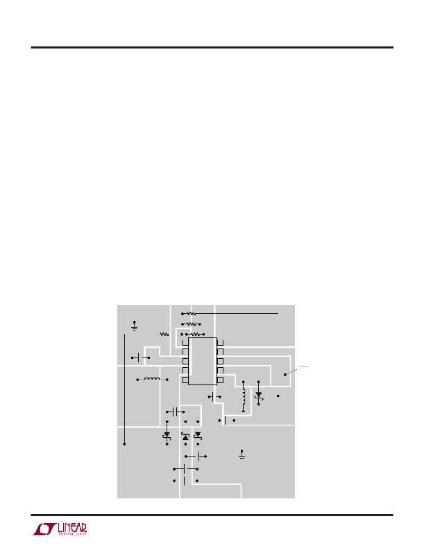
�Layout� Hints�
�The� high� speed� operation� of� the� LT1947� mandates� careful�
�attention� to� layout� for� proper� performance.� Be� sure� to� keep�
�input� capacitor� C1� as� close� as� possible� to� the� IC� and�
�minimize� trace� area� and� length� at� the� SW� and� FB� pins.�
�Always� use� a� ground� plane� under� the� switching� regulator�
�to� minimize� interplane� coupling.� Figure� 2� shows� the� rec-�
�ommended� component� placement.�
�The� exposed� pad� of� the� MSE� package� must� be� soldered� to�
�the� PCB� and� electrically� connected� to� ground.� Thermal�
�vias� to� a� large� ground� plane� will� lower� the� thermal� resis-�
�tance.�
�Soft-Start�
�For� applications� requiring� soft-start,� a� circuit� consisting� of�
�R� SS� and� C� SS� tied� to� the� SHDN� pin� can� be� used,� as� shown�
�in� Figure� 3.� For� a� combination� of� 33.2k/33nF,� AV� DD� rises�
�to� its� final� value� in� approximately� 3ms.�
�GND�
�R4�
�R1�
�1�
�R2�
�10�
�V� ON�
�C5�
�2�
�3�
�LT1947�
�9�
�8�
�L1�
�4�
�5�
�7�
�6�
�SHDN�
�C1�
�V� IN�
�C6�
�C3�
�L2�
�V� IN�
�D2�
�AV� DD�
�D1�
�D3�
�C2�
�C4�
�D4�
�GND�
�V� OFF�
�1947� F02�
�Figure� 2.� Recommended� Component� Placement�
�1947fa�
�7�
�相关PDF资料 |
PDF描述 |
|---|---|
| X5045M8I | IC CPU SUPRV 4K EE RST HI 8MSOP |
| MIC9131YM TR | IC CTRLR DC-DC PWM HV HS 16-SOIC |
| SPX29302T5-L | IC REG LDO ADJ 3A TO263-5 |
| VI-JWJ-EZ-B1 | CONVERTER MOD DC/DC 36V 25W |
| MIC9130YQS TR | IC CTRLR DC-DC PWM HV HS 16-QSOP |
相关代理商/技术参数 |
参数描述 |
|---|---|
| LT1948 | 制造商:LINEAR 制造商全称:LINEAR 功能描述:DC/DC Converter for TFT-LCD Panels |
| LT1948EMS8 | 制造商:LINER 制造商全称:Linear Technology 功能描述:DC/DC Converter for TFT-LCD Panels |
| LT1949 | 制造商:LINER 制造商全称:Linear Technology 功能描述:1.4A, 1.5MHz Synchronous Step-Up DC/DC Converter with Output Disconnect |
| LT1949-1 | 制造商:LINER 制造商全称:Linear Technology 功能描述:1.4A, 1.5MHz Synchronous Step-Up DC/DC Converter with Output Disconnect |
| LT1949-1EMS8 | 功能描述:IC REG BOOST ADJ 1A 8MSOP RoHS:否 类别:集成电路 (IC) >> PMIC - 稳压器 - DC DC 开关稳压器 系列:- 标准包装:20 系列:SIMPLE SWITCHER® 类型:降压(降压) 输出类型:固定 输出数:1 输出电压:12V 输入电压:4 V ~ 60 V PWM 型:电压模式 频率 - 开关:52kHz 电流 - 输出:1A 同步整流器:无 工作温度:-40°C ~ 125°C 安装类型:通孔 封装/外壳:16-DIP(0.300",7.62mm) 包装:管件 供应商设备封装:16-DIP 其它名称:*LM2575HVN-12LM2575HVN-12 |
发布紧急采购,3分钟左右您将得到回复。