- 您现在的位置:买卖IC网 > PDF目录53672 > LT1948EMS8#TR (LINEAR TECHNOLOGY CORP) 1.5 A SWITCHING REGULATOR, 3600 kHz SWITCHING FREQ-MAX, PDSO8 PDF资料下载
参数资料
| 型号: | LT1948EMS8#TR |
| 厂商: | LINEAR TECHNOLOGY CORP |
| 元件分类: | 稳压器 |
| 英文描述: | 1.5 A SWITCHING REGULATOR, 3600 kHz SWITCHING FREQ-MAX, PDSO8 |
| 封装: | PLASTIC, MSOP-8 |
| 文件页数: | 3/4页 |
| 文件大小: | 207K |
| 代理商: | LT1948EMS8#TR |
LT1948
3
PI FU CTIO S
UU
U
FB1 (Pin 1): Feedback Pin for First Switcher. Connect
resistor divider tap here. Set AVDD according to AVDD =
1.26V(1 + R1/R2).
CT (Pin 2): Timing Capacitor Pin. Connect a 22nF capacitor
from CT to ground to program a 3ms delay from FB1
reaching 1.26V to VON turning on.
SW1 (Pin 3): AVDD Switch Node. Connect inductor and D1
here (see Figure 1). Minimize trace area at this pin to keep
EMI down.
GND (Pin 4): Ground. Connect directly to local ground
plane.
VIN (Pin 5): Input Supply Pin. Must be bypassed with a
ceramic capacitor close to the pin.
SW2 (Pin 6): VO2 Switch Node. Connect inductor and D2
here. Minimize trace area at this pin to keep EMI down.
VO2 (Pin 7): Sense Pin for 23V Output. Connect to VO2
output capacitor. This node is also internally connected to
the emitter of Q3 (see Block Diagram), the high side switch
between VO2 and VON.
VON (Pin 8): This is the Delayed 23V Output. VON becomes
23V after the internal timer times out.
To best understand operation of the LT1948, please refer
to the LT1948 Block Diagram. The device contains two
switching regulators, a timer and a high side switch. Three
outputs can be generated: an adjustable AVDD output, a
charge-pumped inversion of the AVDD output, called VOFF,
and a 23V/15mA output, called VON. Q3 keeps VON off for
an externally set time interval, set by a capacitor connected
to the CT pin.
The switching frequency of both switchers is 3MHz, set
internally. The switchers are current mode and are inter-
nally compensated. The main AVDD switcher is current
limited at 1.5A, while the second VON switcher is limited to
800mA. They share the same 1.26V reference voltage.
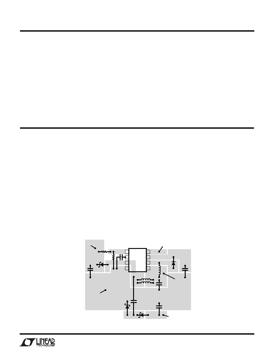
1948 F02
1
2
8
7
3
4
6
5
L3
R1
R2
C1
D1
VON
VIN
VOFF
D4B
D3A
L1–L2
C4
C3
D2
C2
C6
GND
AVDD
OPERATIO
U
Figure 2. Recommended Component Placement
When the input voltage is below approximately 2.4V, an
undervoltage lockout circuit disables switching.
When AVDD is less than its final voltage, Q4 is turned on,
holding the CT pin at ground. When AVDD reaches final
value, Q4 lets go of the CT pin, allowing the 5.5A current
source to charge the external capacitor, CT. When the
voltage on the CT pin reaches 1.25V, Q3 turns on, connect-
ing VO2 to VON. Capacitor value can be calculated using
the following formula:
C = (5.5
A tDELAY)/1.25V
A 22nF capacitor results in approximately 3ms of delay.
相关PDF资料 |
PDF描述 |
|---|---|
| LT253A | SPECIALTY ANALOG CIRCUIT, PDSO4 |
| LT3464DICE | 0.14 A SWITCHING REGULATOR, UUC8 |
| LTC1174IS8-3.3#TRPBF | SWITCHING REGULATOR, PDSO8 |
| LTC1174IS8-3.3#TR | SWITCHING REGULATOR, PDSO8 |
| LTC1325CS | BATTERY CHARGE CONTROLLER, 111 kHz SWITCHING FREQ-MAX, PDSO18 |
相关代理商/技术参数 |
参数描述 |
|---|---|
| LT1949 | 制造商:LINER 制造商全称:Linear Technology 功能描述:1.4A, 1.5MHz Synchronous Step-Up DC/DC Converter with Output Disconnect |
| LT1949-1 | 制造商:LINER 制造商全称:Linear Technology 功能描述:1.4A, 1.5MHz Synchronous Step-Up DC/DC Converter with Output Disconnect |
| LT1949-1EMS8 | 功能描述:IC REG BOOST ADJ 1A 8MSOP RoHS:否 类别:集成电路 (IC) >> PMIC - 稳压器 - DC DC 开关稳压器 系列:- 标准包装:20 系列:SIMPLE SWITCHER® 类型:降压(降压) 输出类型:固定 输出数:1 输出电压:12V 输入电压:4 V ~ 60 V PWM 型:电压模式 频率 - 开关:52kHz 电流 - 输出:1A 同步整流器:无 工作温度:-40°C ~ 125°C 安装类型:通孔 封装/外壳:16-DIP(0.300",7.62mm) 包装:管件 供应商设备封装:16-DIP 其它名称:*LM2575HVN-12LM2575HVN-12 |
| LT1949-1EMS8#PBF | 功能描述:IC REG BOOST ADJ 1A 8MSOP RoHS:是 类别:集成电路 (IC) >> PMIC - 稳压器 - DC DC 开关稳压器 系列:- 标准包装:20 系列:SIMPLE SWITCHER® 类型:降压(降压) 输出类型:固定 输出数:1 输出电压:12V 输入电压:4 V ~ 60 V PWM 型:电压模式 频率 - 开关:52kHz 电流 - 输出:1A 同步整流器:无 工作温度:-40°C ~ 125°C 安装类型:通孔 封装/外壳:16-DIP(0.300",7.62mm) 包装:管件 供应商设备封装:16-DIP 其它名称:*LM2575HVN-12LM2575HVN-12 |
| LT1949-1EMS8#TR | 功能描述:IC REG BOOST ADJ 1A 8MSOP RoHS:否 类别:集成电路 (IC) >> PMIC - 稳压器 - DC DC 开关稳压器 系列:- 标准包装:20 系列:SIMPLE SWITCHER® 类型:降压(降压) 输出类型:固定 输出数:1 输出电压:12V 输入电压:4 V ~ 60 V PWM 型:电压模式 频率 - 开关:52kHz 电流 - 输出:1A 同步整流器:无 工作温度:-40°C ~ 125°C 安装类型:通孔 封装/外壳:16-DIP(0.300",7.62mm) 包装:管件 供应商设备封装:16-DIP 其它名称:*LM2575HVN-12LM2575HVN-12 |
发布紧急采购,3分钟左右您将得到回复。