参数资料
| 型号: | LT1949IS8#TRPBF |
| 厂商: | Linear Technology |
| 文件页数: | 5/8页 |
| 文件大小: | 0K |
| 描述: | IC REG BOOST ADJ 1A 8SOIC |
| 标准包装: | 2,500 |
| 类型: | 升压(升压) |
| 输出类型: | 可调式 |
| 输出数: | 1 |
| 输出电压: | 1.24 V ~ 30 V |
| 输入电压: | 1.7 V ~ 12 V |
| PWM 型: | 电流模式 |
| 频率 - 开关: | 600kHz |
| 电流 - 输出: | 1A |
| 同步整流器: | 无 |
| 工作温度: | -40°C ~ 85°C |
| 安装类型: | 表面贴装 |
| 封装/外壳: | 8-SOIC(0.154",3.90mm 宽) |
| 包装: | 带卷 (TR) |
| 供应商设备封装: | 8-SOIC |
�� �
�
�LT1949-1�
�BLOCK� DIAGRA�
�LBI�
�1.24V�
�REFERENCE�
�FB�
�+�
�g� m�
�V� C�
�1�
�7�
�+�
�LBO�
�8�
�V� OUT�
�R1�
�2�
�–�
�ERROR�
�AMPLIFIER�
�BIAS�
�+�
�–�
�A1�
�200mV�
�ENABLE�
�–�
�A4�
�SHUTDOWN�
�SHDN�
�3�
�(EXTERNAL)�
�FB�
�COMPARATOR�
�SW�
�R2�
�(EXTERNAL)�
�RAMP�
�FF�
�DRIVER�
�5�
�GENERATOR�
�+�
�Σ�
�+�
�R�
�A2�
�COMPARATOR�
�S�
�Q�
�+�
�Q3�
�1.1MHz�
�OSCILLATOR�
�A=2�
�–�
�4�
�0.06� ?�
�1949-1� BD�
�GND�
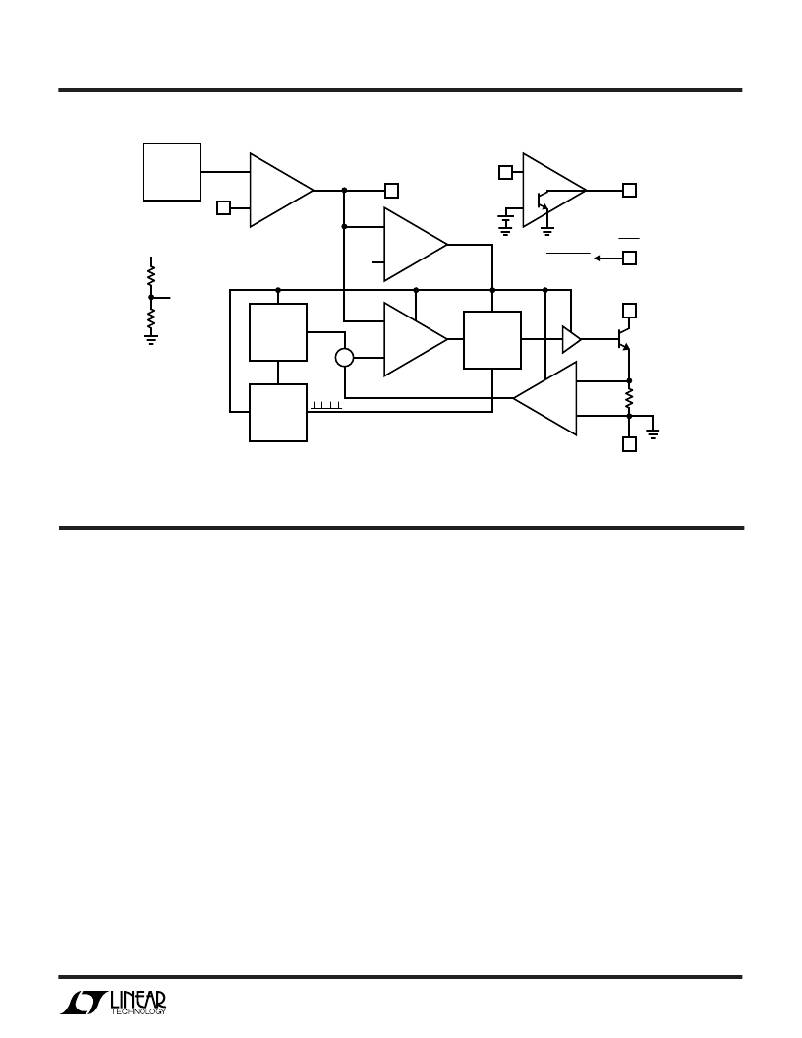
�Figure� 3.� LT1949-1� Block� Diagram�
�OPERATIO�
�The� LT1949-1� is� a� current� mode,� fixed� frequency� step-up�
�DC/DC� converter� with� an� internal� 1A� NPN� power� transis-�
�tor.� Operation� can� best� be� understood� by� referring� to� the�
�Block� Diagram.�
�At� the� beginning� of� each� oscillator� cycle,� the� flip-flop� is� set�
�and� the� switch� is� turned� on.� Current� in� the� switch� ramps�
�up� until� the� voltage� at� A2’s� positive� input� reaches� the� V� C�
�pin� voltage,� causing� A2’s� output� to� change� state� and� the�
�switch� to� be� turned� off.� The� signal� at� A2’s� positive� input� is�
�a� summation� of� a� signal� representing� switch� current� and�
�a� ramp� generator� (introduced� to� avoid� subharmonic� oscil-�
�lations� at� duty� factors� greater� than� 50%).� If� the� load�
�increases,� V� OUT� (and� FB)� will� drop� slightly� and� the� error�
�amplifier� will� drive� V� C� to� a� higher� voltage,� causing� current�
�in� the� switch� to� increase.� In� this� way,� the� error� amplifier�
�drives� the� V� C� pin� to� the� voltage� necessary� to� satisfy� the�
�load.� Frequency� compensation� is� provided� by� an� external�
�series� RC� network� connected� between� the� V� C� pin� and�
�Layout� Hints�
�The� LT1949-1� switches� current� at� high� speed,� mandating�
�careful� attention� to� layout� for� proper� performance.� You�
�will� not� get� advertised� performance� with� careless� layouts.�
�Figure� 4� shows� recommended� component� placement� for�
�a� boost� (step-up)� converter.� Follow� this� closely� in� your� PC�
�layout.� Note� the� direct� path� of� the� switching� loops.� Input�
�capacitor� C1� must� be� placed� close� (<� 5mm)� to� the� IC�
�package.� As� little� as� 10mm� of� wire� or� PC� trace� from� C� IN� to�
�V� IN� will� cause� problems� such� as� inability� to� regulate� or�
�oscillation.�
�The� ground� terminal� of� output� capacitor� C2� should� tie�
�close� to� Pin� 4� of� the� LT1949-1.� Doing� this� reduces� dI/dt� in�
�the� ground� copper� which� keeps� high� frequency� spikes� to�
�a� minimum.� The� DC/DC� converter� ground� should� tie� to� the�
�PC� board� ground� plane� at� one� place� only,� to� avoid� intro-�
�ducing� dI/dt� in� the� ground� plane.�
�ground.�
�5�
�相关PDF资料 |
PDF描述 |
|---|---|
| LT1950IGN#TRPBF | IC REG CTRLR PWM CM 16-SSOP |
| LT1952IGN-1#PBF | IC REG CTRLR ISO PWM CM 16-SSOP |
| LT1956IFE-5#TRPBF | IC REG BUCK 5V 1.5A 16TSSOP |
| LT1959IR#TR | IC REG BUCK ADJ 4.5A D2PAK |
| LT1961IMS8E#TRPBF | IC REG BOOST ADJ 1.5A 8MSOP |
相关代理商/技术参数 |
参数描述 |
|---|---|
| LT1950 | 制造商:LINER 制造商全称:Linear Technology 功能描述:Single Switch PWM Controller with Auxiliary Boost Converter |
| LT1950EGN | 功能描述:IC REG CTRLR PWM CM 16-SSOP RoHS:否 类别:集成电路 (IC) >> PMIC - 稳压器 - DC DC 切换控制器 系列:- 标准包装:2,500 系列:- PWM 型:电流模式 输出数:1 频率 - 最大:500kHz 占空比:96% 电源电压:4 V ~ 36 V 降压:无 升压:是 回扫:无 反相:无 倍增器:无 除法器:无 Cuk:无 隔离:无 工作温度:-40°C ~ 125°C 封装/外壳:24-WQFN 裸露焊盘 包装:带卷 (TR) |
| LT1950EGN#PBF | 功能描述:IC REG CTRLR PWM CM 16-SSOP RoHS:是 类别:集成电路 (IC) >> PMIC - 稳压器 - DC DC 切换控制器 系列:- 标准包装:2,500 系列:- PWM 型:电流模式 输出数:1 频率 - 最大:500kHz 占空比:96% 电源电压:4 V ~ 36 V 降压:无 升压:是 回扫:无 反相:无 倍增器:无 除法器:无 Cuk:无 隔离:无 工作温度:-40°C ~ 125°C 封装/外壳:24-WQFN 裸露焊盘 包装:带卷 (TR) |
| LT1950EGN#TR | 功能描述:IC REG CTRLR PWM CM 16-SSOP RoHS:否 类别:集成电路 (IC) >> PMIC - 稳压器 - DC DC 切换控制器 系列:- 标准包装:2,500 系列:- PWM 型:电流模式 输出数:1 频率 - 最大:500kHz 占空比:96% 电源电压:4 V ~ 36 V 降压:无 升压:是 回扫:无 反相:无 倍增器:无 除法器:无 Cuk:无 隔离:无 工作温度:-40°C ~ 125°C 封装/外壳:24-WQFN 裸露焊盘 包装:带卷 (TR) |
| LT1950EGN#TRPBF | 功能描述:IC REG CTRLR PWM CM 16-SSOP RoHS:是 类别:集成电路 (IC) >> PMIC - 稳压器 - DC DC 切换控制器 系列:- 标准包装:2,500 系列:- PWM 型:电流模式 输出数:1 频率 - 最大:500kHz 占空比:96% 电源电压:4 V ~ 36 V 降压:无 升压:是 回扫:无 反相:无 倍增器:无 除法器:无 Cuk:无 隔离:无 工作温度:-40°C ~ 125°C 封装/外壳:24-WQFN 裸露焊盘 包装:带卷 (TR) |
发布紧急采购,3分钟左右您将得到回复。