- 您现在的位置:买卖IC网 > PDF目录13860 > LT1976HFE#PBF (Linear Technology)IC REG BUCK ADJ 1.5A 16TSSOP PDF资料下载
参数资料
| 型号: | LT1976HFE#PBF |
| 厂商: | Linear Technology |
| 文件页数: | 4/28页 |
| 文件大小: | 0K |
| 描述: | IC REG BUCK ADJ 1.5A 16TSSOP |
| 标准包装: | 95 |
| 类型: | 降压(降压) |
| 输出类型: | 可调式 |
| 输出数: | 1 |
| 输出电压: | 1.2 V ~ 54 V |
| 输入电压: | 3.3 V ~ 60 V |
| PWM 型: | 电流模式,混合 |
| 频率 - 开关: | 200kHz |
| 电流 - 输出: | 1.5A |
| 同步整流器: | 无 |
| 工作温度: | -40°C ~ 150°C |
| 安装类型: | 表面贴装 |
| 封装/外壳: | 16-TSSOP(0.173",4.40mm)裸露焊盘 |
| 包装: | 管件 |
| 供应商设备封装: | 16-TSSOP-EP |
第1页第2页第3页当前第4页第5页第6页第7页第8页第9页第10页第11页第12页第13页第14页第15页第16页第17页第18页第19页第20页第21页第22页第23页第24页第25页第26页第27页第28页
�� �
�
�LT1976/LT1976B�
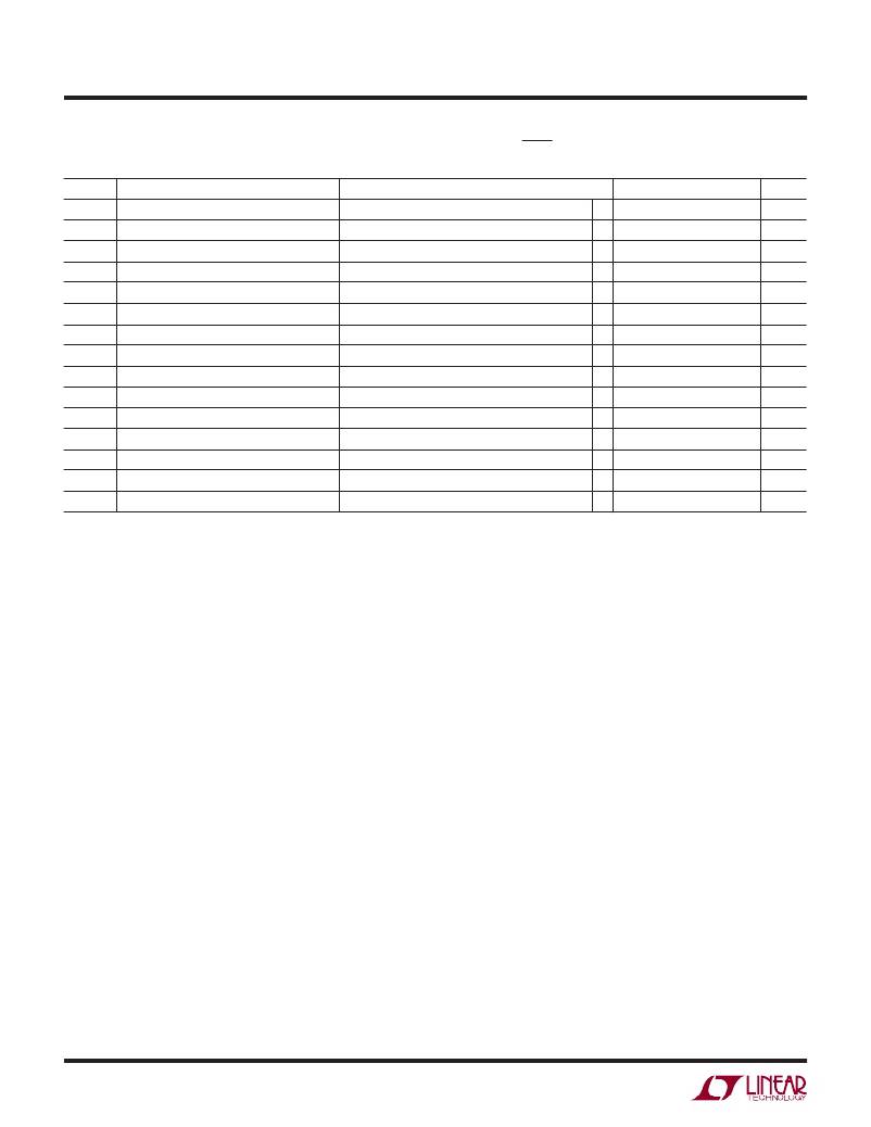
�ELECTRICAL� CHARACTERISTICS� The� ●� denotes� the� specifications� which� apply� over� the� full� –40� °� C� to� 140� °� C�
�operating� temperature� range,� otherwise� specifications� are� at� T� J� =� 25� °� C.� V� IN� =� 12V,� SHDN� =� 12V,� BOOST� =� 15.3V,� BIAS� =� 5V,�
�FB/PGFB� =� 1.25V,� C� SS� /SYNC� =� 0V� unless� otherwise� noted.�
�SYMBOL�
�PARAMETER�
�CONDITIONS�
�MIN�
�TYP�
�MAX�
�UNITS�
�I� PK�
�SW� Current� Limit�
�2.4�
�A�
�Switch� On� Resistance� (Note� 9)�
�●�
�0.2�
�0.6�
�Ω�
�Switching� Frequency�
�BOOST� =� OPEN�
�●�
�150�
�200�
�260�
�kHz�
�Maximum� Duty� Cycle�
�90�
�92�
�%�
�Minimum� SYNC� Amplitude�
�1.5�
�2.0�
�V�
�SYNC� Frequency� Range�
�SYNC� Input� Impedance�
�SYNC� =� 0.5V�
�230�
�600�
�85�
�kHz�
�k� Ω�
�I� CSS�
�I� PGFB�
�C� SS� Current� Threshold� (Note� 10)�
�PGFB� Input� Current�
�7�
�13�
�25�
�20�
�100�
�μ� A�
�nA�
�V� PGFB�
�I� CT�
�PGFB� Voltage� Threshold� (Note� 11)�
�C� T� Source� Current� (Note� 11)�
�●�
�●�
�87�
�1.5�
�90�
�3.6�
�93�
�5.5�
�%�
�μ� A�
�C� T� Sink� Current� (Note� 11)�
�1�
�2�
�mA�
�V� CT�
�C� T� Voltage� Threshold� (Note� 11)�
�PG� Leakage� (Note� 11)�
�PG� Sink� Current� (Note� 11)�
�PG� =� 12V�
�PGFB� =� 1V,� PG� =� 400mV�
�1.16�
�120�
�1.2�
�0.1�
�200�
�1.26�
�1�
�V�
�μ� A�
�μ� A�
�Note� 1:� Stresses� beyond� those� listed� under� Absolute� Maximum� Ratings�
�may� cause� permanent� damage� to� the� device.� Exposure� to� any� Absolute�
�Maximum� Rating� condition� for� extended� periods� may� affect� device�
�reliability� and� lifetime.�
�Note� 2:� The� LT1976EFE/LT1976BEFE� are� guaranteed� to� meet� performance�
�specifications� from� 0� °� C� to� 125� °� C� junction� temperature.� Specifications� over�
�the� –40� °� C� to� 125� °� C� operating� junction� temperature� range� are� assured� by�
�design,� characterization� and� correlation� with� statistical� process� controls.�
�The� LT1976IFE/LT1976BIFE/LT1976HFE� are� guaranteed� and� tested� over�
�the� full� –40� °� C� to� 125� °� C� operating� junction� temperature� range.� The�
�LT1976HFE� is� also� tested� to� the� LT1976HFE� electrical� characteristics� table�
�at� 140� °� C� operating� junction� temperature.� High� junction� temperatures�
�degrade� operating� lifetimes.�
�Note� 3:� Minimum� input� voltage� is� defined� as� the� voltage� where� switching�
�starts.� Actual� minimum� input� voltage� to� maintain� a� regulated� output� will�
�depend� upon� output� voltage� and� load� current.� See� Applications�
�Information.�
�Note� 4:� Supply� input� current� is� the� quiescent� current� drawn� by� the� input�
�pin.� Its� typical� value� depends� on� the� voltage� on� the� BIAS� pin� and� operating�
�state� of� the� LT1976.� With� the� BIAS� pin� at� 0V,� all� of� the� quiescent� current�
�required� to� operate� the� LT1976� will� be� provided� by� the� V� IN� pin.� With� the�
�Note� 5:� Minimum� BIAS� voltage� is� the� voltage� on� the� BIAS� pin� when� I� BIAS� is�
�sourced� into� the� pin.�
�Note� 6:� This� is� the� minimum� voltage� across� the� boost� capacitor� needed� to�
�guarantee� full� saturation� of� the� internal� power� switch.�
�Note� 7:� Boost� current� is� the� current� flowing� into� the� BOOST� pin� with� the�
�pin� held� 3.3V� above� input� voltage.� It� flows� only� during� switch� on� time.�
�Note� 8:� Gain� is� measured� with� a� V� C� swing� from� 1.15V� to� 750mV.�
�Note� 9:� Switch� on� resistance� is� calculated� by� dividing� V� IN� to� SW� voltage� by�
�the� forced� current� (1.5A� LT1976,� 1.2A� LT1976B).� See� Typical� Performance�
�Characteristics� for� the� graph� of� switch� voltage� at� other� currents.�
�Note� 10:� The� C� SS� threshold� is� defined� as� the� value� of� current� sourced� into�
�the� C� SS� pin� which� results� in� an� increase� in� sink� current� from� the� V� C� pin.�
�See� the� Soft-Start� section� in� Applications� Information.�
�Note� 11:� The� PGFB� threshold� is� defined� as� the� percentage� of� V� REF� voltage�
�which� causes� the� current� source� output� of� the� C� T� pin� to� change� from�
�sinking� (below� threshold)� to� sourcing� current� (above� threshold).� When�
�sourcing� current,� the� voltage� on� the� C� T� pin� rises� until� it� is� clamped�
�internally.� When� the� clamp� is� activated,� the� output� of� the� PG� pin� will� be� set�
�to� a� high� impedance� state.� When� the� C� T� clamp� is� inactive� the� PG� pin� will�
�be� set� active� low� with� a� current� sink� capability� of� 200� μ� A.�
�BIAS� voltage� above� its� minimum� input� voltage,� a� portion� of� the� total�
�quiescent� current� will� be� supplied� by� the� BIAS� pin.� Supply� sleep� current�
�for� the� LT1976� is� defined� as� the� quiescent� current� during� the� “sleep”�
�portion� of� Burst� Mode� operation.� See� Applications� Information� for�
�determining� application� supply� currents.�
�1976bfg�
�4�
�相关PDF资料 |
PDF描述 |
|---|---|
| MAX6716AUTWGD1+T | IC SUPERVISOR MPU SOT23-6 |
| HSM22DSXN | CONN EDGECARD 44POS DIP .156 SLD |
| EMM12DTBD | CONN EDGECARD 24POS R/A .156 SLD |
| LT1269CSW#TR | IC REG BUCK INV FLYBK 4A 20SOIC |
| MAX6716AUTWED5+T | IC SUPERVISOR MPU SOT23-6 |
相关代理商/技术参数 |
参数描述 |
|---|---|
| LT1976IFE | 功能描述:IC REG BUCK ADJ 1.5A 16TSSOP RoHS:否 类别:集成电路 (IC) >> PMIC - 稳压器 - DC DC 开关稳压器 系列:- 设计资源:Design Support Tool 标准包装:1 系列:- 类型:升压(升压) 输出类型:固定 输出数:1 输出电压:3V 输入电压:0.75 V ~ 2 V PWM 型:- 频率 - 开关:- 电流 - 输出:100mA 同步整流器:是 工作温度:-40°C ~ 85°C 安装类型:表面贴装 封装/外壳:SOT-23-5 细型,TSOT-23-5 包装:剪切带 (CT) 供应商设备封装:TSOT-23-5 其它名称:AS1323-BTTT-30CT |
| LT1976IFE#PBF | 功能描述:IC REG BUCK ADJ 1.5A 16TSSOP RoHS:是 类别:集成电路 (IC) >> PMIC - 稳压器 - DC DC 开关稳压器 系列:- 标准包装:250 系列:- 类型:降压(降压) 输出类型:固定 输出数:1 输出电压:1.2V 输入电压:2.05 V ~ 6 V PWM 型:电压模式 频率 - 开关:2MHz 电流 - 输出:500mA 同步整流器:是 工作温度:-40°C ~ 85°C 安装类型:表面贴装 封装/外壳:6-UFDFN 包装:带卷 (TR) 供应商设备封装:6-SON(1.45x1) 产品目录页面:1032 (CN2011-ZH PDF) 其它名称:296-25628-2 |
| LT1976IFE#PBF | 制造商:Linear Technology 功能描述:DC/DC Converter IC |
| LT1976IFE#TR | 功能描述:IC REG BUCK ADJ 1.5A 16TSSOP RoHS:否 类别:集成电路 (IC) >> PMIC - 稳压器 - DC DC 开关稳压器 系列:- 设计资源:Design Support Tool 标准包装:1 系列:- 类型:升压(升压) 输出类型:固定 输出数:1 输出电压:3V 输入电压:0.75 V ~ 2 V PWM 型:- 频率 - 开关:- 电流 - 输出:100mA 同步整流器:是 工作温度:-40°C ~ 85°C 安装类型:表面贴装 封装/外壳:SOT-23-5 细型,TSOT-23-5 包装:剪切带 (CT) 供应商设备封装:TSOT-23-5 其它名称:AS1323-BTTT-30CT |
| LT1976IFE#TRPBF | 功能描述:IC REG BUCK ADJ 1.5A 16TSSOP RoHS:是 类别:集成电路 (IC) >> PMIC - 稳压器 - DC DC 开关稳压器 系列:- 设计资源:Design Support Tool 标准包装:1 系列:- 类型:升压(升压) 输出类型:固定 输出数:1 输出电压:3V 输入电压:0.75 V ~ 2 V PWM 型:- 频率 - 开关:- 电流 - 输出:100mA 同步整流器:是 工作温度:-40°C ~ 85°C 安装类型:表面贴装 封装/外壳:SOT-23-5 细型,TSOT-23-5 包装:剪切带 (CT) 供应商设备封装:TSOT-23-5 其它名称:AS1323-BTTT-30CT |
发布紧急采购,3分钟左右您将得到回复。