参数资料
| 型号: | LT1993CUD-10#PBF |
| 厂商: | Linear Technology |
| 文件页数: | 4/16页 |
| 文件大小: | 0K |
| 描述: | IC DIFF AMP/ADC DRVR 16-QFN |
| 标准包装: | 121 |
| 放大器类型: | 差分 |
| 电路数: | 2 |
| 输出类型: | 差分 |
| 转换速率: | 1100 V/µs |
| -3db带宽: | 700MHz |
| 电流 - 输入偏压: | 5µA |
| 电压 - 输入偏移: | 1000µV |
| 电流 - 电源: | 100mA |
| 电流 - 输出 / 通道: | 45mA |
| 电压 - 电源,单路/双路(±): | 4 V ~ 5.5 V,±2 V ~ 2.5 V |
| 工作温度: | 0°C ~ 70°C |
| 安装类型: | 表面贴装 |
| 封装/外壳: | 16-WFQFN 裸露焊盘 |
| 供应商设备封装: | 16-QFN-EP(3x3) |
| 包装: | 管件 |
| 产品目录页面: | 1322 (CN2011-ZH PDF) |
LT1993-10
12
199310fb
APPLICATIO S I FOR ATIO
WU
U
Single-Ended to Differential Operation
The LT1993-10’s performance with single-ended inputs
is comparable to its performance with differential inputs.
This excellent single-ended performance is largely due
to the internal topology of the LT1993-10. Referring to
the block diagram, if the +INA and +INB pins are driven
with a single-ended signal (while –INA and –INB are tied
to AC ground), then the +OUT and –OUT pins are driven
differentially without any voltage swing needed from
amplier C. Single-ended to differential conversion using
more conventional topologies suffers from performance
limitations due to the common mode amplier.
Driving ADCs
The LT1993-10 has been specically designed to interface
directly with high speed Analog to Digital Converters
(ADCs). In general, these ADCs have differential inputs,
with an input impedance of 1k or higher. In addition, there
is generally some form of lowpass or bandpass ltering just
prior to the ADC to limit input noise at the ADC, thereby
improving system signal to noise ratio. Both the unltered
and ltered outputs of the LT1993-10 can easily drive the
high impedance inputs of these differential ADCs. If the
ltered outputs are used, then cutoff frequency and the
type of lter can be tailored for the specic application if
needed.
Wideband Applications
(Using the +OUT and –OUT Pins)
In applications where the full bandwidth of the LT1993-10
is desired, the unltered output pins (+OUT and –OUT)
should be used. They have a low output impedance;
therefore, gain is unaffected by output load. Capacitance
in excess of 5pF placed directly on the unltered outputs
results in additional peaking and reduced performance.
When driving an ADC directly, a small series resistance
is recommended between the LT1993-10’s outputs and
the ADC inputs (Figure 4). This resistance helps eliminate
any resonances associated with bond wire inductances of
either the ADC inputs or the LT1993-10’s outputs. A value
between 10
Ω and 25Ω gives excellent results.
Filtered Applications
(Using the +OUTFILTERED and –OUTFILTERED Pins)
Filtering at the output of the LT1993-10 is often desired
to provide either anti-aliasing or improved signal to noise
ratio. To simplify this ltering, the LT1993-10 includes an
additional pair of differential outputs (+OUTFILTERED and
–OUTFILTERED) which incorporate an internal lowpass
lter network with a –3dB bandwidth of 175MHz (Figure
5). These pins each have an output impedance of 25
Ω. In-
ternal capacitances are 12pF to VEE on each ltered output,
plus an additional 12pF capacitor connected differentially
between the two ltered outputs. This resistor/capaci-
tor combination creates ltered outputs that look like a
series 25
Ω resistor with a 36pF capacitor shunting each
ltered output to AC ground, giving a –3dB bandwidth of
175MHz.
199310 F04
LT1993-10
–OUT
+OUT
8
5
10
9 TO 259
10
9 TO 259
ADC
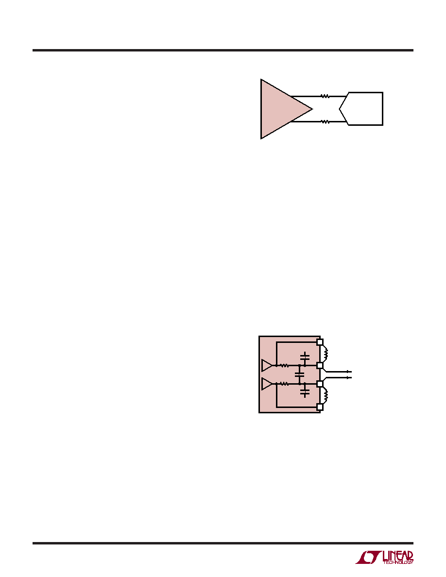
Figure 4. Adding Small Series R at LT1993-10 Output
The lter cutoff frequency is easily modied with just a
few external components. To increase the cutoff frequency,
simply add 2 equal value resistors, one between +OUT and
+OUTFILTERED and the other between –OUT and –OUTFIL-
TERED (Figure 6). These resistors are in parallel with the
internal 25
Ω resistor, lowering the overall resistance and
increasing lter bandwidth. To double the lter bandwidth,
for example, add two external 25
Ω resistors to lower
the series resistance to 12.5
Ω. The 36pF of capacitance
remains unchanged, so lter bandwidth doubles.
Figure 5. LT1993-10 Internal Filter Topology –3dB BW ≈175MHz
VEE
199310 F05
25
9
25
9
12pF
LT1993-10
–OUT
+OUT
25
9
25
9
12pF
–OUTFILTERED
FILTERED OUTPUT
(350MHz)
+OUTFILTERED
8
7
6
5
相关PDF资料 |
PDF描述 |
|---|---|
| LT6600CS8-20#PBF | IC AMP DIFF LP FLTR 20MHZ 8-SOIC |
| LT6234IDD#PBF | IC OP AMP DUAL 60MHZ R-R 8-DFN |
| TMM-102-01-G-S | CONN HEADER 2POS SNGL 2MM T/H |
| AD8032AR | IC OPAMP VF R-R DUAL LP 8SOIC |
| AD8042ARZ | IC OPAMP VF R-R DUAL LP 8SOIC |
相关代理商/技术参数 |
参数描述 |
|---|---|
| LT1993CUD-2 | 制造商:Linear Technology 功能描述:SP Amp DIFF AMP Single 5.5V 16-Pin QFN EP 制造商:Linear Technology 功能描述:DIFF-AMPLIFIER, 800MHZ, 1.1KV/US, QFN-16, No. of Amplifiers:2, Input Offset Voltage:1mV, Gain dB Max:6.3dB, Bandwidth:800MHz, Amplifier Case Style:QFN, No. of Pins:16, Supply Voltage Range:4V to 5.5V, Slew Rate:1.1kV/s, MSL:- |
| LT1993CUD-2#PBF | 功能描述:IC DIFF AMP/ADC DRVR 16-QFN RoHS:是 类别:集成电路 (IC) >> Linear - Amplifiers - Instrumentation 系列:- 标准包装:50 系列:- 放大器类型:J-FET 电路数:2 输出类型:- 转换速率:3.5 V/µs 增益带宽积:1MHz -3db带宽:- 电流 - 输入偏压:30pA 电压 - 输入偏移:2000µV 电流 - 电源:200µA 电流 - 输出 / 通道:- 电压 - 电源,单路/双路(±):7 V ~ 36 V,±3.5 V ~ 18 V 工作温度:0°C ~ 70°C 安装类型:通孔 封装/外壳:8-DIP(0.300",7.62mm) 供应商设备封装:8-PDIP 包装:管件 |
| LT1993CUD-2#TR | 制造商:Linear Technology 功能描述:DIFF-AMPLIFIER, 800MHZ, 1.1KV/US, QFN-16, No. of Amplifiers:2, Input Offset Volt 制造商:Linear Technology 功能描述:DIFF-AMPLIFIER, 800MHZ, 1.1KV/US, QFN-16, No. of Amplifiers:2, Input Offset Voltage:1mV, Gain dB Max:6.3dB, Bandwidth:800MHz, Amplifier Case Style:QFN, No. of Pins:16, Supply Voltage Range:4V to 5.5V, Slew Rate:1.1kV/s, MSL:- |
| LT1993CUD-2#TRPBF | 功能描述:IC DIFF AMP/ADC DRVR 16-QFN RoHS:是 类别:集成电路 (IC) >> Linear - Amplifiers - Instrumentation 系列:- 标准包装:50 系列:- 放大器类型:J-FET 电路数:2 输出类型:- 转换速率:3.5 V/µs 增益带宽积:1MHz -3db带宽:- 电流 - 输入偏压:30pA 电压 - 输入偏移:2000µV 电流 - 电源:200µA 电流 - 输出 / 通道:- 电压 - 电源,单路/双路(±):7 V ~ 36 V,±3.5 V ~ 18 V 工作温度:0°C ~ 70°C 安装类型:通孔 封装/外壳:8-DIP(0.300",7.62mm) 供应商设备封装:8-PDIP 包装:管件 |
| LT1993CUD-4 | 制造商:Linear Technology 功能描述:DIFF-AMPLIFIER, 900MHZ, 1.1KV/US, QFN-16, No. of Amplifiers:2, Input Offset Voltage:1mV, Gain dB Max:12.4dB, Bandwidth:900MHz, Amplifier Case Style:QFN, No. of Pins:16, Supply Voltage Range:4V to 5.5V, Slew Rate:1.1kV/s, MSL:- |
发布紧急采购,3分钟左右您将得到回复。