参数资料
| 型号: | LT1993IUD-4#TRPBF |
| 厂商: | Linear Technology |
| 文件页数: | 5/16页 |
| 文件大小: | 0K |
| 描述: | IC DIFF AMP/ADC DRVR 16-QFN |
| 标准包装: | 2,500 |
| 放大器类型: | 差分 |
| 电路数: | 2 |
| 输出类型: | 差分 |
| 转换速率: | 1100 V/µs |
| -3db带宽: | 900MHz |
| 电流 - 输入偏压: | 5µA |
| 电压 - 输入偏移: | 1000µV |
| 电流 - 电源: | 100mA |
| 电流 - 输出 / 通道: | 45mA |
| 电压 - 电源,单路/双路(±): | 4 V ~ 5.5 V,±2 V ~ 2.5 V |
| 工作温度: | -40°C ~ 85°C |
| 安装类型: | 表面贴装 |
| 封装/外壳: | 16-WFQFN 裸露焊盘 |
| 供应商设备封装: | 16-QFN-EP(3x3) |
| 包装: | 带卷 (TR) |
LT1993-4
13
19934fa
APPLICATIO S I FOR ATIO
WU
U
To decrease lter bandwidth, add two external capaci-
tors, one from +OUTFILTERED to ground, and the other
from –OUTFILTERED to ground. A single differential
capacitor connected between +OUTFILTERED and –OUT-
FILTERED can also be used, but since it is being driven
differentially it will appear at each ltered output as a
single-ended capacitance of twice the value. To halve the
lter bandwidth, for example, two 36pF capacitors could
be added (one from each ltered output to ground). Al-
ternatively one 18pF capacitor could be added between
the ltered outputs, again halving the lter bandwidth.
Combinations of capacitors could be used as well; a three
capacitor solution of 12pF from each ltered output to
ground plus a 12pF capacitor between the ltered outputs
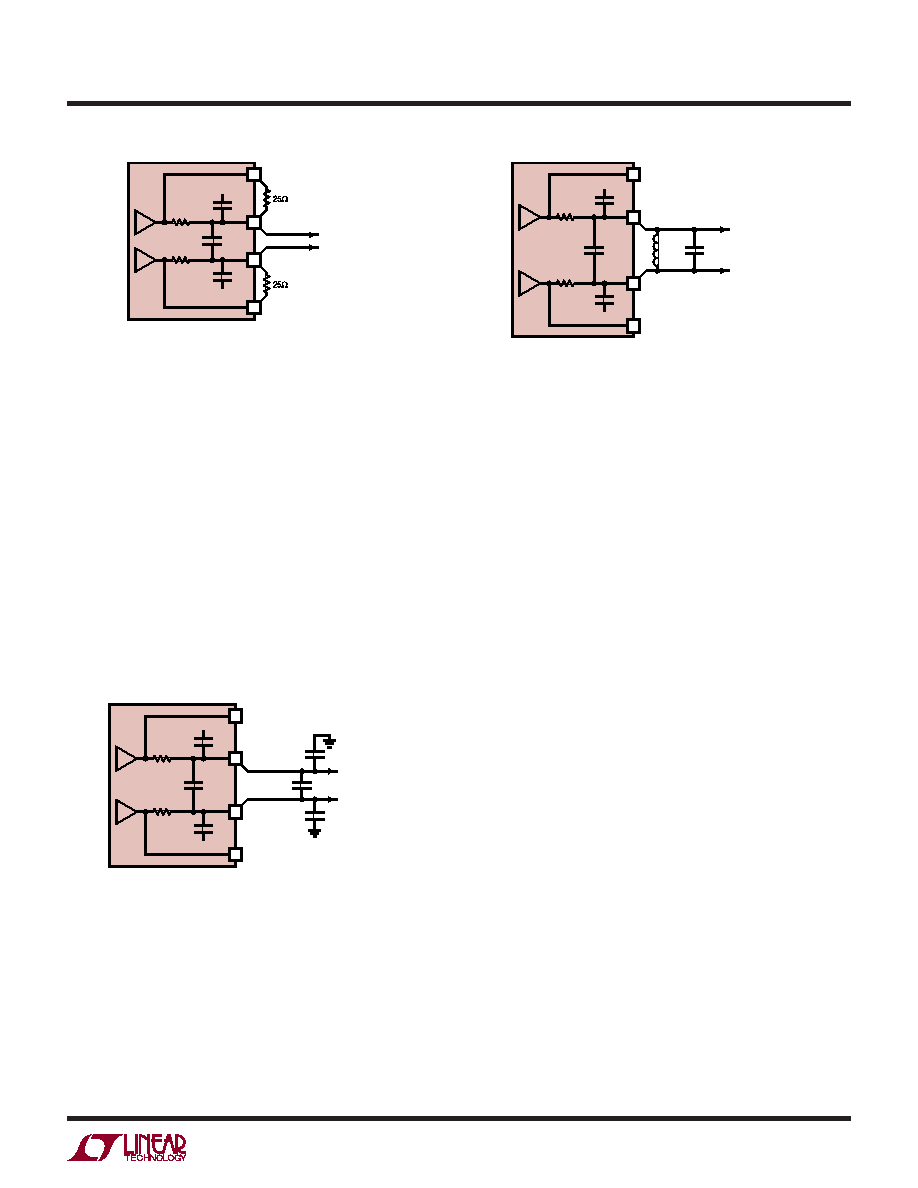
would also halve the lter bandwidth (Figure 7).
Bandpass ltering is also easily implemented with just a
few external components. An additional 120pF and 39nH,
each added differentially between +OUTFILTERED and
–OUTFILTERED creates a bandpass lter with a 71MHz
center frequency, –3dB points of 55MHz and 87MHz, and
1.6dB of insertion loss (Figure 8).
Figure 6. LT1993-4 Internal Filter Topology Modied for
2x Filter Bandwidth (2 External Resistors)
Output Common Mode Adjustment
The LT1993-4’s output common mode voltage is set by the
VOCM pin. It is a high-impedance input, capable of setting
the output common mode voltage anywhere in a range
from 1.1V to 3.6V. Bandwidth of the VOCM pin is typically
300MHz, so for applications where the VOCM pin is tied to
a DC bias voltage, a 0.1F capacitor at this pin is recom-
mended. For best distortion performance, the voltage at
the VOCM pin should be between 1.8V and 2.6V.
When interfacing with most ADCs, there is generally a VOCM
output pin that is at about half of the supply voltage of the
ADC. For 5V ADCs such as the LTC17XX family, this VOCM
output pin should be connected directly (with the addition
of a 0.1F capacitor) to the input VOCM pin of the LT1993-4.
For 3V ADCs such as the LTC22XX families, the LT1993-
4 will function properly using the 1.65V from the ADC’s
VCM reference pin, but improved Spurious Free Dynamic
Range (SFDR) and distortion performance can be achieved
by level-shifting the LTC22XX’s VCM reference voltage up
to at least 1.8V. This can be accomplished as shown in
Figure 9 by using a resistor divider between the LTC22XX’s
VCMoutput pin and VCC and then bypassing the LT1993-4’s
VOCMpin with a 0.1F capacitor. For a common mode volt-
age above 1.9V, AC coupling capacitors are recommended
between the LT1993-4 and the LTC22XX ADC because of
the input voltage range constraints of the ADC.
Figure 7. LT1993-4 Internal Filter Topology Modied for
1/2x Filter Bandwidth (3 External Capacitors)
VEE
19934 F06
12pF
LT1993-4
–OUT
+OUT
12pF
25
25
12pF
–OUTFILTERED
FILTERED OUTPUT
(350MHz)
+OUTFILTERED
8
7
6
5
VEE
19934 F07
12pF
LT1993-4
–OUT
+OUT
12pF
–OUTFILTERED
+OUTFILTERED
8
7
6
5
FILTERED OUTPUT
(87.5MHz)
25
9
25
9
Figure 8. LT1993-4 Output Filter Topology Modied for Bandpass
Filtering (1 External Inductor, 1 External Capacitor)
VEE
19934 F08
12pF
LT1993-4
–OUT
+OUT
12pF
120pF
39nH
–OUTFILTERED
+OUTFILTERED
8
7
6
5
FILTERED OUTPUT
(71MHz BANDPASS,
–3dB @ 55MHz/87MHz)
25
9
25
9
相关PDF资料 |
PDF描述 |
|---|---|
| LTC6910-3CTS8#TRPBF | IC PGA DIGITAL R-R I/O TSOT23-8 |
| LTC6910-2CTS8#TRPBF | IC PGA DIGITAL R-R I/O TSOT23-8 |
| 1-534237-2 | CONN RECEPT 14POS .100 VERT AU |
| LTC6910-1CTS8#TRPBF | IC PGA DIGITAL R-R I/O TSOT23-8 |
| 1-535541-0 | CONN RECEPT 12POS .100 VERT AU |
相关代理商/技术参数 |
参数描述 |
|---|---|
| LT1994 | 制造商:LINER 制造商全称:Linear Technology 功能描述:Precision, Low Power Rail-to-Rail Input/Output |
| LT1994CDD | 制造商:Linear Technology 功能描述:SC-Amps/High Speed, 70MHz Low Noise/Distortion Differential Amplifer |
| LT1994CDD#PBF | 功能描述:IC DIFF AMP/DRIVER LN 8-DFN RoHS:是 类别:集成电路 (IC) >> Linear - Amplifiers - Instrumentation 系列:- 产品培训模块:Differential Circuit Design Techniques for Communication Applications 标准包装:1 系列:- 放大器类型:RF/IF 差分 电路数:1 输出类型:差分 转换速率:9800 V/µs 增益带宽积:- -3db带宽:2.9GHz 电流 - 输入偏压:3µA 电压 - 输入偏移:- 电流 - 电源:40mA 电流 - 输出 / 通道:- 电压 - 电源,单路/双路(±):3 V ~ 3.6 V 工作温度:-40°C ~ 85°C 安装类型:表面贴装 封装/外壳:16-VQFN 裸露焊盘,CSP 供应商设备封装:16-LFCSP-VQ 包装:剪切带 (CT) 产品目录页面:551 (CN2011-ZH PDF) 其它名称:ADL5561ACPZ-R7CT |
| LT1994CDD#PBF | 制造商:Linear Technology 功能描述:Operational Amplifier (Op-Amp) IC 制造商:Linear Technology 功能描述:IC, DIFFERENTIAL AMP, 70MHZ, 65V/ uS DFN8 |
| LT1994CDD#TR | 制造商:Linear Technology 功能描述:DIFF-AMPLIFIER, 70MHZ, 65V/US, DFN-8, No. of Amplifiers:1, Input Offset Voltage: 制造商:Linear Technology 功能描述:DIFF-AMPLIFIER, 70MHZ, 65V/US, DFN-8, No. of Amplifiers:1, Input Offset Voltage:2mV, Bandwidth:70MHz, Amplifier Case Style:DFN, No. of Pins:8, Supply Voltage Range:2.375V to 12.6V, Slew Rate:65V/s, Supply Current:14.8mA, MSL:- , RoHS Compliant: No |
发布紧急采购,3分钟左右您将得到回复。