- 您现在的位置:买卖IC网 > PDF目录1823 > LT3010MPMS8E-5#TRPBF (Linear Technology)IC REG LDO 5V 50MA 8-MSOP PDF资料下载
参数资料
| 型号: | LT3010MPMS8E-5#TRPBF |
| 厂商: | Linear Technology |
| 文件页数: | 4/18页 |
| 文件大小: | 0K |
| 描述: | IC REG LDO 5V 50MA 8-MSOP |
| 标准包装: | 2,500 |
| 稳压器拓扑结构: | 正,固定式 |
| 输出电压: | 5V |
| 输入电压: | 最高 80 V |
| 电压 - 压降(标准): | 0.3V @ 50mA |
| 稳压器数量: | 1 |
| 电流 - 输出: | 50mA |
| 电流 - 限制(最小): | 60mA |
| 工作温度: | -55°C ~ 125°C |
| 安装类型: | 表面贴装 |
| 封装/外壳: | 8-TSSOP,8-MSOP(0.118",3.00mm 宽)裸露焊盘 |
| 供应商设备封装: | 8-MSOP-EP |
| 包装: | 带卷 (TR) |
�� �
�
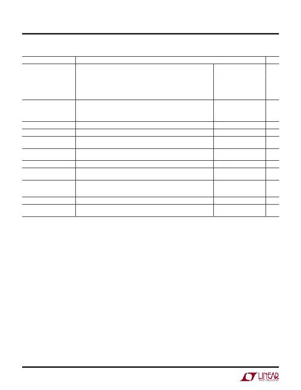
�LT3010/LT3010-5�
�ELECTRICAL� CHARACTERISTICS� (LT3010H)� The� l� denotes� the� specifications� which� apply� over� the� –40°C� to�
�140°C operating temperatur� e� range,� otherwise� specifications� are� at� T� A� =� 25°C.�
�PARAMETER�
�Dropout� Voltage�
�V� IN� =� V� OUT(NOMINAL)�
�(Notes� 4,� 5)�
�GND� Pin� Current�
�V� IN� =� V� OUT(NOMINAL)�
�(Notes� 4,� 6)�
�Output� Voltage� Noise�
�ADJ� Pin� Bias� Current�
�CONDITIONS�
�I� LOAD� =� 1mA�
�I� LOAD� =� 1mA�
�I� LOAD� =� 10mA�
�I� LOAD� =� 10mA�
�I� LOAD� =� 50mA�
�I� LOAD� =� 50mA�
�I� LOAD� =� 0mA�
�I� LOAD� =� 1mA�
�I� LOAD� =� 10mA�
�I� LOAD� =� 50mA�
�C� OUT� =� 10μF,� I� LOAD� =� 250mA,� BW� =� 10Hz� to� 100kHz�
�(Note� 7)�
�l�
�l�
�l�
�l�
�l�
�l�
�l�
�MIN�
�TYP�
�100�
�200�
�300�
�30�
�100�
�400�
�1.8�
�100�
�50�
�MAX�
�150�
�220�
�260�
�380�
�370�
�600�
�80�
�200�
�750�
�3.5�
�100�
�UNITS�
�mV�
�mV�
�mV�
�mV�
�mV�
�mV�
�μA�
�μA�
�μA�
�mA�
�μV� RMS�
�nA�
�Shutdown� Threshold�
�SHDN� Pin� Current�
�(Note� 8)�
�V� OUT� =� Off� to� On�
�V� OUT� =� On� to� Off�
�V� SHDN� =� 0V�
�V� SHDN� =� 6V�
�l�
�l�
�0.3�
�1.3�
�0.8�
�0.5�
�0.1�
�2�
�2�
�0.5�
�V�
�V�
�μA�
�μA�
�Quiescent Current in Shutdown� V� IN� =� 6V,� V� SHDN� =� 0V�
�1�
�5�
�μA�
�Ripple� Rejection�
�LT3010�
�LT3010-5�
�V� IN� =� 7V(Avg),� V� RIPPLE� =� 0.5V� P-P� ,� f� RIPPLE� =� 120Hz,� I� LOAD� =� 50mA�
�V� IN� =� 7V(Avg),� V� RIPPLE� =� 0.5V� P-P� ,� f� RIPPLE� =� 120Hz,� I� LOAD� =� 50mA�
�65�
�60�
�75�
�68�
�dB�
�dB�
�Current� Limit�
�V� IN� =� 7V,� V� OUT� =� 0V�
�LT3010-5� V� IN� =� 6V,� Δ� V� OUT� =� –0.1V�
�LT3010� (Note� 2)� V� IN� =� 4.25V,� Δ� V� OUT� =� –0.1V�
�l�
�l�
�l�
�55�
�55�
�140�
�mA�
�mA�
�mA�
�Input� Reverse� Leakage� Current� V� IN� =� –80V,� V� OUT� =� 0V�
�l�
�6�
�mA�
�Reverse� Output� Current�
�(Note� 9)�
�LT3010-5� V� OUT� =� 5V,� V� IN� <� 5V�
�LT3010� (Note� 2)� V� OUT� =� 1.275V,� V� IN� <� 1.275V�
�10�
�8�
�20�
�15�
�μA�
�μA�
�Note� 1:� Stresses� beyond� those� listed� under� Absolute� Maximum� Ratings�
�may� cause� permanent� damage� to� the� device.� Exposure� to� any� Absolute�
�Maximum� Rating� condition� for� extended� periods� may� affect� device�
�reliability� and� lifetime.�
�Note� 2:� The� LT3010� (adjustable� version)� is� tested� and� specified� for� these�
�conditions� with� the� ADJ� pin� connected� to� the� OUT� pin.�
�Note� 3:� Operating� conditions� are� limited� by� maximum� junction�
�temperature.� The� regulated� output� voltage� specification� will� not� apply�
�for� all� possible� combinations� of� input� voltage� and� output� current.� When�
�operating� at� maximum� input� voltage,� the� output� current� range� must� be�
�limited.� When� operating� at� maximum� output� current,� the� input� voltage�
�range� must� be� limited.�
�Note� 4:� To� satisfy� requirements� for� minimum� input� voltage,� the� LT3010�
�(adjustable� version)� is� tested� and� specified� for� these� conditions� with� an�
�external� resistor� divider� (249k� bottom,� 392k� top)� for� an� output� voltage� of�
�3.3V.� The� external� resistor� divider� will� add� a� 5μA� DC� load� on� the� output.�
�Note� 5:� Dropout� voltage� is� the� minimum� input� to� output� voltage� differential�
�needed� to� maintain� regulation� at� a� specified� output� current.� In� dropout,� the�
�output� voltage� will� be� equal� to� (V� IN� –� V� DROPOUT� ).�
�Note� 6:� GND� pin� current� is� tested� with� V� IN� =� V� OUT� (nominal)� and� a� current�
�source� load.� This� means� the� device� is� tested� while� operating� in� its� dropout�
�region.� This� is� the� worst-case� GND� pin� current.� The� GND� pin� current� will�
�decrease� slightly� at� higher� input� voltages.�
�Note� 7:� ADJ� pin� bias� current� flows� into� the� ADJ� pin.�
�Note� 8:� SHDN� pin� current� flows� out� of� the� SHDN� pin.�
�Note� 9:� Reverse� output� current� is� tested� with� the� IN� pin� grounded� and� the�
�OUT� pin� forced� to� the� rated� output� voltage.� This� current� flows� into� the� OUT�
�pin� and� out� the� GND� pin.�
�Note� 10:� The� LT3010E� is� guaranteed� to� meet� performance� specifications�
�from� 0°C� to� 125°C� operating� junction� temperature.� Specifications� over�
�the� –40°C� to� 125°C� operating� junction� temperature� range� are� assured� by�
�design,� characterization� and� correlation� with� statistical� process� controls.�
�The� LT3010H� is� tested� to� the� LT3010H� Electrical� Characteristics� table� at�
�140°C� operating� junction� temperature.� The� LT3010MP� is� 100%� tested� and�
�guaranteed� over� the� –55°C� to� 125°C� operating� junction� temperature� range.�
�High� junction� temperatures� degrade� operating� lifetimes.� Operating� lifetime�
�is� derated� at� junction� temperatures� greater� than� 125°C.�
�Note� 11:� This� IC� includes� overtemperature� protection� that� is� intended�
�to� protect� the� device� during� momentary� overload� conditions.� Junction�
�temperature� will� exceed� 125°C� (LT3010E� and� LT3010MP)� or� 140°C�
�(LT3010H)� when� overtemperature� protection� is� active.� Continuous�
�operation� above� the� specified� maximum� operating� junction� temperature�
�may� impair� device� reliability.�
�30105fe�
�4�
�相关PDF资料 |
PDF描述 |
|---|---|
| LT3011HMSE#TRPBF | IC REG LDO ADJ 50MA 12-MSOP |
| LT3012HFE#TRPBF | IC REG LDO ADJ .2A 16-TSSOP |
| LT3013MPFE#PBF | IC REG LDO ADJ .25A 16-TSSOP |
| LT3014HVIS5#TRPBF | IC REG LDO ADJ 20MA SOT23-5 |
| LT3015MPQ-5#TRPBF | IC REG LDO -5V 1.5A DDPAK-5 |
相关代理商/技术参数 |
参数描述 |
|---|---|
| LT3011 | 制造商:LINER 制造商全称:Linear Technology 功能描述:50mA, 3V to 80V Low Dropout Micropower Linear Regulator with PWRGD |
| LT3011EDD | 制造商:LINER 制造商全称:Linear Technology 功能描述:50mA, 3V to 80V Low Dropout Micropower Linear Regulator with PWRGD |
| LT3011EDD#PBF | 功能描述:IC REG LDO ADJ 50MA 10-DFN RoHS:是 类别:集成电路 (IC) >> PMIC - 稳压器 - 线性 系列:- 产品培训模块:MIC5365/66 Ultra-small LDO Regulators 标准包装:1 系列:- 稳压器拓扑结构:正,固定式 输出电压:3V 输入电压:最高 5.5V 电压 - 压降(标准):0.155V @ 150mA 稳压器数量:1 电流 - 输出:150mA 电流 - 限制(最小):200mA 工作温度:-40°C ~ 125°C 安装类型:表面贴装 封装/外壳:4-UDFN 裸露焊盘,4-TMLF? 供应商设备封装:4-TMLF?(1x1) 包装:Digi-Reel® 其它名称:576-3192-6 |
| LT3011EDD#TRPBF | 功能描述:IC REG LDO ADJ 50MA 10-DFN RoHS:是 类别:集成电路 (IC) >> PMIC - 稳压器 - 线性 系列:- 产品培训模块:More Information on LDOs 标准包装:50 系列:- 稳压器拓扑结构:正,固定式 输出电压:3.3V 输入电压:最高 15V 电压 - 压降(标准):1.1V @ 800mA 稳压器数量:1 电流 - 输出:800mA 电流 - 限制(最小):800mA 工作温度:0°C ~ 125°C 安装类型:表面贴装 封装/外壳:TO-263-4,D²Pak(3 引线+接片),TO-263AA 供应商设备封装:D2PAK-3 包装:管件 |
| LT3011EDDPBF | 制造商:LINER 制造商全称:Linear Technology 功能描述:50mA, 3V to 80V Low Dropout Micropower Linear Regulator with PWRGD |
发布紧急采购,3分钟左右您将得到回复。