参数资料
| 型号: | LT3015IQ-15#PBF |
| 厂商: | Linear Technology |
| 文件页数: | 14/26页 |
| 文件大小: | 0K |
| 描述: | IC REG LDO -15V 1.5A DDPAK-5 |
| 标准包装: | 50 |
| 稳压器拓扑结构: | 负,固定式 |
| 输出电压: | -15V |
| 输入电压: | 可下调至 -30V |
| 电压 - 压降(标准): | 0.41V @ 1.5A |
| 稳压器数量: | 1 |
| 电流 - 输出: | 1.5A |
| 电流 - 限制(最小): | 1.7A |
| 工作温度: | -40°C ~ 125°C |
| 安装类型: | 表面贴装 |
| 封装/外壳: | TO-263-6,D²Pak(5 引线+接片),TO-263BA |
| 供应商设备封装: | DDPAK/TO-263-5 |
| 包装: | 管件 |
�� �
�
�LT3015� Series�
�PIN� FUNCTIONS�
�(DFN/MSOP/Q/T)�
�IN� (Pins� 1,� 2,� Exposed� Pad� Pin� 9� /� 1,� 2,� 3,� 4,� Exposed�
�Pad� Pin� 13� /� 3,� Tab� /� 3,� Tab� ):� Input.� These� pins� supply�
�power� to� the� regulator.� The� Tab� of� the� DD-Pak,� TO-220� and�
�the� exposed� backside� pad� of� the� DFN� and� MSOP� packages�
�is� an� electrical� connection� to� IN� and� to� the� device’s� sub-�
�strate.� For� proper� electrical� and� thermal� performance,� tie�
�all� IN� pins� together� and� tie� IN� to� the� exposed� backside� or�
�Tab� of� the� relevant� package� on� the� PCB.� See� the� Applica-�
�tions� Information� Section� for� thermal� considerations� and�
�calculating� junction� temperature.� The� LT3015� requires�
�a� bypass� capacitor� at� IN.� In� general,� a� battery’s� output�
�impedance� rises� with� frequency,� so� include� a� bypass� ca-�
�pacitor� in� battery� powered� applications.� An� input� bypass�
�capacitor� in� the� range� of� 1μF� to� 10μF� generally� suffices,�
�but� applications� with� large� load� transients� may� require�
�higher� input� capacitance� to� prevent� input� supply� droop�
�and� prevent� the� regulator� from� entering� dropout.�
�SHDN� (Pin� 3� /� 5� /� 1� /� 1):� Shutdown.� Use� the� SHDN� pin� to�
�put� the� LT3015� into� a� micropower� shutdown� state.� The�
�SHDN� function� is� bi-directional,� allowing� use� of� either�
�positive� or� negative� logic.� The� SHDN� pin� threshold� volt-�
�ages� are� referenced� to� GND.� The� output� of� the� LT3015� is�
�OFF� if� the� SHDN� pin� is� pulled� typically� within� ±0.73V� of�
�GND.� Driving� the� SHDN� pin� typically� more� than� ±1.21V�
�turns� the� LT3015� ON.� Drive� the� SHDN� pin� with� either� a�
�logic� gate� or� with� open� collector/drain� logic� using� a� pull-up�
�resistor.� The� resistor� supplies� the� pull-up� current� of� the�
�open� collector/drain� gate,� typically� several� microamperes.�
�The� typical� SHDN� pin� current� is� 2.8μA� out� of� the� pin� (for�
�negative� logic)� or� 17μA� into� the� pin� (for� positive� logic).� If�
�the� SHDN� function� is� unused,� connect� the� SHDN� pin� to�
�V� IN� to� turn� the� device� ON.� If� the� SHDN� pin� is� floated,� then�
�the� LT3015� is� OFF.� A� parasitic� diode� exists� between� SHDN�
�and� IN� of� the� LT3015.� Therefore,� do� not� drive� the� SHDN�
�pin� more� than� 0.3V� below� IN� during� normal� operation� or�
�during� a� fault� condition.� The� SHDN� pin� can� also� be� used�
�to� set� a� programmable� undervoltage� lockout� (UVLO)�
�threshold� for� the� regulator� input� supply.�
�It� has� a� typical� bias� current� of� 30nA� that� flows� into� the�
�pin.� The� ADJ� pin� reference� voltage� is� –1.22V� referred� to�
�GND,� and� the� output� voltage� range� is� –1.22V� to� –29.5V.� A�
�parasitic� substrate� diode� exists� between� ADJ� and� IN� of� the�
�LT3015.� Therefore,� do� not� drive� ADJ� more� than� 0.3V� below�
�IN� during� normal� operation� or� during� a� fault� condition.�
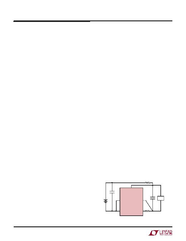
�SENSE� (Pin� 6� /� 8� /� 4� /� 4):� Sense.� For� the� fixed� voltage� ver-�
�sions� of� the� LT3015� (LT3015-2.5/LT3015-3/LT3015-3.3/�
�LT3015-5/LT3015-12/LT3015-15),� the� SENSE� pin� connects�
�to� the� non-inverting� input� of� the� error� amplifier� through�
�an� internal� resistor� divider� network.� Optimum� regulation�
�is� obtained� when� the� SENSE� pin� is� connected� to� the� OUT�
�pin� of� the� regulator.� In� critical� applications,� small� voltage�
�drops� are� caused� by� the� resistance� (R� P� )� of� PCB� traces�
�between� the� regulator� and� the� load.� These� drops� can� be�
�eliminated� by� connecting� the� SENSE� pin� to� the� output� at�
�the� load� as� shown� in� Figure� 1� (Kelvin� Sense� Connection).�
�Note� that� the� voltage� drop� across� the� external� PCB� traces�
�will� add� to� the� dropout� voltage� of� the� regulator.� The� SENSE�
�pin� bias� current� is� 100μA� at� the� nominal� output� voltage.� A�
�parasitic� diode� exists� between� SENSE� and� IN� of� the� LT3015.�
�Therefore,� do� not� drive� SENSE� more� than� 0.3V� below� IN�
�during� normal� operation� or� during� a� fault� condition.�
�OUT� (Pins� 7,� 8� /� 9,� 10,� 11,� 12� /� 5� /� 5):� Output.� These�
�pins� supply� power� to� the� load.� Tie� all� OUT� pins� together�
�for� best� performance.� Use� a� minimum� output� capacitor�
�of� 10μF� with� an� ESR� less� than� 500mΩ� to� prevent� oscil-�
�lations.� Large� load� transient� applications� require� larger�
�output� capacitors� to� limit� peak� voltage� transients.� See�
�the� Applications� Information� section� for� more� information�
�on� output� capacitance.� A� parasitic� substrate� diode� exists�
�between� OUT� and� IN� of� the� LT3015.� Therefore,� do� not� drive�
�OUT� more� than� 0.3V� below� IN� during� normal� operation� or�
�during� a� fault� condition.�
�R� P�
�GND�
�GND� (Pins� 4,� 5� /� 6,� 7� /� 2� /� 2):� Ground.� Tie� all� GND� pin(s)�
�together� and� tie� the� bottom� of� the� output� voltage� setting�
�resistor� divider� directly� to� the� GND� pin(s)� for� optimum�
�load� regulation� performance.�
�V� IN�
�SHDN�
�IN�
�LT3015-XX�
�SENSE�
�OUT�
�R� P�
�LOAD�
�ADJ� (Pin� 6� /� 8� /� 4� /� 4):� Adjust.� For� the� adjustable� voltage�
�version,� this� pin� is� the� error� amplifier’s� non-inverting� input.�
�3015� F01�
�Figure� 1.� Kelvin� Sense� Connection�
�3015fb�
�14�
�相关PDF资料 |
PDF描述 |
|---|---|
| LT3015IQ-12#PBF | IC REG LDO -12V 1.5A DDPAK-5 |
| LT1764AET-3.3#06PBF | IC REG LDO 3.3V 3A TO220-5 |
| IDT72V51256L6BB | IC FLOW CTRL MULTI QUEUE 256-BGA |
| LFXP10E-4F388C | IC FPGA 9.7KLUTS 244I/O 388-BGA |
| LFXP10E-3F388I | IC FPGA 9.7KLUTS 244I/O 388-BGA |
相关代理商/技术参数 |
参数描述 |
|---|---|
| LT3015IQ-2.5#PBF | 功能描述:IC REG LDO -2.5V 1.5A DDPAK-5 RoHS:是 类别:集成电路 (IC) >> PMIC - 稳压器 - 线性 系列:- 标准包装:1 系列:- 稳压器拓扑结构:正,固定式 输出电压:3V 输入电压:2.3 V ~ 5.5 V 电压 - 压降(标准):0.035V @ 150mA 稳压器数量:2 电流 - 输出:150mA 电流 - 限制(最小):300mA 工作温度:-40°C ~ 125°C 安装类型:表面贴装 封装/外壳:6-UFDFN 裸露焊盘,6-TMLF? 供应商设备封装:6-TMLF?(1.6x1.6) 包装:Digi-Reel® 产品目录页面:1104 (CN2011-ZH PDF) 其它名称:576-3018-6 |
| LT3015IQ-2.5#TRPBF | 功能描述:IC REG LDO -2.5V 1.5A DDPAK-5 RoHS:是 类别:集成电路 (IC) >> PMIC - 稳压器 - 线性 系列:- 标准包装:1 系列:- 稳压器拓扑结构:正,固定式 输出电压:3V 输入电压:2.3 V ~ 5.5 V 电压 - 压降(标准):0.035V @ 150mA 稳压器数量:2 电流 - 输出:150mA 电流 - 限制(最小):300mA 工作温度:-40°C ~ 125°C 安装类型:表面贴装 封装/外壳:6-UFDFN 裸露焊盘,6-TMLF? 供应商设备封装:6-TMLF?(1.6x1.6) 包装:Digi-Reel® 产品目录页面:1104 (CN2011-ZH PDF) 其它名称:576-3018-6 |
| LT3015IQ-3#PBF | 功能描述:IC REG LDO -3V 1.5A DDPAK-5 RoHS:是 类别:集成电路 (IC) >> PMIC - 稳压器 - 线性 系列:- 标准包装:1 系列:- 稳压器拓扑结构:正,固定式 输出电压:3V 输入电压:2.3 V ~ 5.5 V 电压 - 压降(标准):0.035V @ 150mA 稳压器数量:2 电流 - 输出:150mA 电流 - 限制(最小):300mA 工作温度:-40°C ~ 125°C 安装类型:表面贴装 封装/外壳:6-UFDFN 裸露焊盘,6-TMLF? 供应商设备封装:6-TMLF?(1.6x1.6) 包装:Digi-Reel® 产品目录页面:1104 (CN2011-ZH PDF) 其它名称:576-3018-6 |
| LT3015IQ-3#TRPBF | 功能描述:IC REG LDO -3V 1.5A DDPAK-5 RoHS:是 类别:集成电路 (IC) >> PMIC - 稳压器 - 线性 系列:- 标准包装:1 系列:- 稳压器拓扑结构:正,固定式 输出电压:3V 输入电压:2.3 V ~ 5.5 V 电压 - 压降(标准):0.035V @ 150mA 稳压器数量:2 电流 - 输出:150mA 电流 - 限制(最小):300mA 工作温度:-40°C ~ 125°C 安装类型:表面贴装 封装/外壳:6-UFDFN 裸露焊盘,6-TMLF? 供应商设备封装:6-TMLF?(1.6x1.6) 包装:Digi-Reel® 产品目录页面:1104 (CN2011-ZH PDF) 其它名称:576-3018-6 |
| LT3015IQ-3.3#PBF | 功能描述:IC REG LDO -3.3V 1.5A DDPAK-5 RoHS:是 类别:集成电路 (IC) >> PMIC - 稳压器 - 线性 系列:- 标准包装:1 系列:- 稳压器拓扑结构:正,固定式 输出电压:3V 输入电压:2.3 V ~ 5.5 V 电压 - 压降(标准):0.035V @ 150mA 稳压器数量:2 电流 - 输出:150mA 电流 - 限制(最小):300mA 工作温度:-40°C ~ 125°C 安装类型:表面贴装 封装/外壳:6-UFDFN 裸露焊盘,6-TMLF? 供应商设备封装:6-TMLF?(1.6x1.6) 包装:Digi-Reel® 产品目录页面:1104 (CN2011-ZH PDF) 其它名称:576-3018-6 |
发布紧急采购,3分钟左右您将得到回复。