参数资料
| 型号: | LT3020IMS8#PBF |
| 厂商: | Linear Technology |
| 文件页数: | 8/16页 |
| 文件大小: | 0K |
| 描述: | IC REG LDO ADJ .1A 8MSOP |
| 标准包装: | 50 |
| 稳压器拓扑结构: | 正,可调式 |
| 输出电压: | 0.2 V ~ 9.5 V |
| 输入电压: | 0.9 V ~ 10 V |
| 电压 - 压降(标准): | 0.15V @ 100mA |
| 稳压器数量: | 1 |
| 电流 - 输出: | 100mA |
| 电流 - 限制(最小): | 110mA |
| 工作温度: | -40°C ~ 125°C |
| 安装类型: | 表面贴装 |
| 封装/外壳: | 8-TSSOP,8-MSOP(0.118",3.00mm 宽) |
| 供应商设备封装: | 8-MSOP |
| 包装: | 管件 |
�� �
�
�LT3020/LT3020-1.2/�
�LT3020-1.5/LT3020-1.8�
�TYPICAL� PERFOR� A� CE� CHARACTERISTICS�
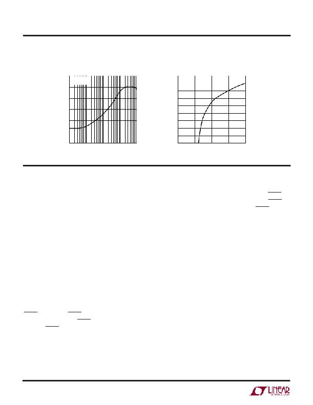
�RMS� Output� Noise� vs� Load�
�Current� (10Hz� to� 100kHz)�
�No-Load� Recovery� Threshold�
�300�
�V� OUT� =� 1.2V�
�C� OUT� =� 2.2� μ� F�
�18�
�16�
�250�
�14�
�200�
�12�
�10�
�150�
�8�
�100�
�6�
�4�
�50�
�2�
�0�
�0.01�
�0.1�
�1� 10�
�100�
�0�
�0�
�5�
�10�
�15�
�20�
�LOAD� CURRENT� (mA)�
�3020� G19�
�PI� FU� CTIO� S�
�OUT� (Pins� 1,� 2):� These� pins� supply� power� to� the� load.� Use�
�a� minimum� output� capacitor� of� 2.2� μ� F� to� prevent� oscillations.�
�Applications� with� large� load� transients� require� larger� out-�
�put� capacitors� to� limit� peak� voltage� transients.� See� the�
�Applications� Information� section� for� more� information� on�
�output� capacitance� and� reverse� output� characteristics.�
�OUT� (Pin� 3,� Fixed� Voltage� Device� Only):� This� pin� is� the�
�sense� point� for� the� internal� resistor� divider.� It� should� be�
�tied� directly� to� the� other� OUT� pins� (1,� 2)� for� best� results.�
�ADJ� (Pin� 3,� Adjustable� Device� Only):� This� pin� is� the�
�inverting� terminal� to� the� error� amplifier.� Its� typical� input�
�bias� current� of� 20nA� flows� out� of� the� pin� (see� curve� of� ADJ�
�Pin� Bias� Current� vs� Temperature� in� the� Typical� Perfor-�
�mance� Characteristics).� The� ADJ� pin� reference� voltage� is�
�200mV� (referred� to� GND).�
�GND� (Pin� 4):� Ground.�
�SHDN� (Pin� 5):� The� SHDN� pin� puts� the� LT3020� into� a� low�
�power� state.� Pulling� the� SHDN� pin� low� turns� the� output� off.�
�Drive� the� SHDN� pin� with� either� logic� or� an� open� collector/�
�drain� device� with� a� pull-up� resistor.� The� pull-up� resistor�
�OUTPUT� OVERSHOOT� (%)�
�3020� G20�
�supplies� the� pull-up� current� to� the� open� collector/drain�
�logic,� normally� several� microamperes,� and� the� SHDN� pin�
�current,� typically� 2.3� μ� A.� If� unused,� connect� the� SHDN� pin�
�to� V� IN� .� The� LT3020� does� not� function� if� the� SHDN� pin� is� not�
�connected.�
�IN� (Pins� 7,� 8):� These� pins� supply� power� to� the� device.� The�
�LT3020� requires� a� bypass� capacitor� at� IN� if� it� is� more� than�
�six� inches� away� from� the� main� input� filter� capacitor.� The�
�output� impedance� of� a� battery� rises� with� frequency,� so�
�include� a� bypass� capacitor� in� battery-powered� circuits.� A�
�bypass� capacitor� in� the� range� of� 2.2� μ� F� to� 10� μ� F� suffices.� The�
�LT3020� withstands� reverse� voltages� on� the� IN� pin� with�
�respect� to� ground� and� the� OUT� pin.� In� the� case� of� a� reversed�
�input,� which� occurs� if� a� battery� is� plugged� in� backwards,�
�the� LT3020� acts� as� if� a� diode� is� in� series� with� its� input.� No�
�reverse� current� flows� into� the� LT3020� and� no� reverse� volt-�
�age� appears� at� the� load.� The� device� protects� itself� and� the�
�load.�
�GND� (Pin� 9,� DD8� Package� Only):� Ground.� Solder� Pin� 9�
�(the� exposed� pad)� to� the� PCB.� Connect� directly� to� Pin� 4� for�
�best� performance.�
�3020fc�
�8�
�相关PDF资料 |
PDF描述 |
|---|---|
| LT1964EDD#TRPBF | IC REG LDO NEG ADJ .2A 8DFN |
| EMM30DTKT | CONN EDGECARD 60POS DIP .156 SLD |
| SPX29151T5-L-1-8 | IC REG LDO 1.8V 1.5A TO263-5 |
| AP130-18YL-13 | IC REG LDO 1.8V .3A SOT89-3 |
| RSM22DTMN-S664 | CONN EDGECARD 44POS R/A .156 |
相关代理商/技术参数 |
参数描述 |
|---|---|
| LT3021 | 制造商:LINER 制造商全称:Linear Technology 功能描述:1.1A, Low Noise, Low Dropout Linear Regulator |
| LT3021-1.2 | 制造商:LINER 制造商全称:Linear Technology 功能描述:500mA, Low Voltage, Very Low Dropout Linear Regulator |
| LT3021-1.5 | 制造商:LINER 制造商全称:Linear Technology 功能描述:500mA, Low Voltage, Very Low Dropout Linear Regulator |
| LT3021-1.8 | 制造商:LINER 制造商全称:Linear Technology 功能描述:500mA, Low Voltage, Very Low Dropout Linear Regulator |
| LT3021EDH | 制造商:Linear Technology 功能描述:LDO Regulator Pos 0.2V to 9.5V 0.5A 16-Pin DFN EP |
发布紧急采购,3分钟左右您将得到回复。