参数资料
| 型号: | LT3029MPMSE#PBF |
| 厂商: | Linear Technology |
| 文件页数: | 3/20页 |
| 文件大小: | 0K |
| 描述: | IC REG LDO ADJ .5A 16MSOP |
| 产品培训模块: | LT3029 - 500mA, Dual Output, 1.2 ~ 19.5V, Linear Regulator |
| 标准包装: | 37 |
| 稳压器拓扑结构: | 正,可调式 |
| 输出电压: | 1.215 V ~ 19.5 V |
| 输入电压: | 1.8 V ~ 20 V |
| 电压 - 压降(标准): | 0.3V @ 500mA |
| 稳压器数量: | 2 |
| 电流 - 输出: | 500mA |
| 电流 - 限制(最小): | 520mA |
| 工作温度: | -55°C ~ 125°C |
| 安装类型: | 表面贴装 |
| 封装/外壳: | 16-TFSOP(0.118",3.00mm 宽)裸露焊盘 |
| 供应商设备封装: | 16-MSOP,裸露焊盘 |
| 包装: | 管件 |
| 产品目录页面: | 1330 (CN2011-ZH PDF) |
�� �
�
�LT3029�
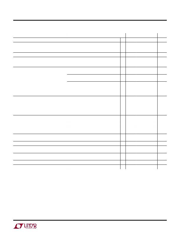
�ELECTRICAL� CHARACTERISTICS� The� l� denotes� the� speci?cations� which� apply� over� the� full� operating�
�temperature� range,� otherwise� speci?cations� are� at� T� A� =� 25°C.� (Note� 2)�
�PARAMETER�
�Minimum� Input� Voltage� (Notes� 3,� 11)�
�CONDITIONS�
�I� LOAD� =� 500mA�
�l�
�MIN�
�TYP�
�1.8�
�MAX�
�2.3�
�UNITS�
�V�
�ADJ1,� ADJ2� Pin� Voltage� (Notes� 3,� 4,� 9)�
�Line� Regulation� (Note� 3)�
�Load� Regulation� (Note� 3)�
�Dropout� Voltage�
�V� IN� =� V� OUT(NOMINAL)�
�(Notes� 5,� 6,� 11)�
�GND� Pin� Current� (per� Channel)�
�V� IN� =� V� OUT(NOMINAL)�
�(Notes� 5,� 7)�
�V� IN� =� 2V,� I� LOAD� =� 1mA�
�2.3V� <� V� IN� <� 20V,� 1mA� <� I� LOAD� <� 500mA� (E,� I,� MP)�
�2.3V� <� V� IN� <� 20V,� 1mA� <� I� LOAD� <� 500mA� (H)�
�ΔV� IN� =� 2V� to� 20V,� I� LOAD� =� 1mA�
�V� IN� =� 2.3V,� ΔI� LOAD� =� 1mA� to� 500mA�
�V� IN� =� 2.3V,� ΔI� LOAD� =� 1mA� to� 500mA� (E,� I,� MP)�
�V� IN� =� 2.3V,� ΔI� LOAD� =� 1mA� to� 500mA� (H)�
�I� LOAD� =� 10mA�
�I� LOAD� =� 10mA�
�I� LOAD� =� 50mA�
�I� LOAD� =� 50mA�
�I� LOAD� =� 100mA�
�I� LOAD� =� 100mA�
�I� LOAD� =� 500mA�
�I� LOAD� =� 500mA�
�I� LOAD� =� 0mA�
�I� LOAD� =� 1mA�
�I� LOAD� =� 50mA�
�I� LOAD� =� 100mA�
�I� LOAD� =� 250mA�
�I� LOAD� =� 500mA�
�l�
�l�
�l�
�l�
�l�
�l�
�l�
�l�
�l�
�l�
�l�
�l�
�l�
�l�
�l�
�1.203�
�1.191�
�1.173�
�1.215�
�1.215�
�1.215�
�0.5�
�2.5�
�0.11�
�0.16�
�0.2�
�0.3�
�55�
�90�
�1.1�
�2�
�4.3�
�10�
�1.227�
�1.239�
�1.239�
�5�
�6�
�15�
�32�
�0.18�
�0.25�
�0.22�
�0.31�
�0.25�
�0.34�
�0.36�
�0.46�
�150�
�250�
�2�
�3.5�
�8�
�16�
�V�
�V�
�V�
�mV�
�mV�
�mV�
�mV�
�V�
�V�
�V�
�V�
�V�
�V�
�V�
�V�
�μA�
�μA�
�mA�
�mA�
�mA�
�mA�
�Output� Voltage� Noise�
�C� OUT� =� 10μF,� C� BYP� =� 10nF,� I� LOAD� =� 500mA,�
�20�
�μV� RMS�
�BW� =� 10Hz� to� 100kHz�
�ADJ1/ADJ2� Pin� Bias� Current�
�ADJ1,� ADJ2� (Notes� 3,� 8)�
�30�
�100�
�nA�
�Shutdown� Threshold�
�SHDN1� /� SHDN2� Pin� Current� (Note� 10)�
�Quiescent� Current� in� Shutdown� (per� Channel)�
�Ripple� Rejection�
�V� OUT� =� Off� to� On�
�V� OUT� =� On� to� Off�
�V� SHDN1� ,� V� SHDN2� =� 0V�
�V� SHDN1� ,� V� SHDN2� =� 20V�
�V� IN� =� 6V,� V� SHDN1� =� 0V,� V� SHDN2� =� 0V�
�V� IN� =� 2.715V� (Avg),� V� RIPPLE� =� 0.5V� P-P� ,�
�l�
�l�
�l�
�l�
�0.20�
�55�
�0.45�
�0.40�
�0�
�0.6�
�0.01�
�67�
�1.1�
�0.5�
�3�
�0.1�
�V�
�V�
�μA�
�μA�
�μA�
�dB�
�f� RIPPLE� =� 120Hz,� I� LOAD� =� 500mA�
�Current� Limit� (Note� 9)�
�V� IN� =� 7V,� V� OUT� =� 0V�
�V� IN� =� 2.3V,� ΔV� OUT� =� –0.1V�
�l�
�520�
�1.5�
�A�
�mA�
�Input� Reverse� Leakage� Current�
�Reverse� Output� Current�
�V� IN� =� –20V,� V� OUT� =� 0V�
�V� OUT� =� 1.215V,� V� IN� =� 0V�
�l�
�0.5�
�1�
�10�
�mA�
�μA�
�Note� 1:� Stresses� beyond� those� listed� under� Absolute� Maximum� Ratings�
�may� cause� permanent� damage� to� the� device.� Exposure� to� any� Absolute�
�Maximum� Rating� condition� for� extended� periods� may� affect� device�
�reliability� and� lifetime.�
�Note� 2:� The� LT3029� is� tested� and� speci?ed� under� pulse� load� conditions�
�such� that� T� J� ≈� T� A� .� The� LT3029E� is� 100%� tested� at� T� A� =� 25°C.� Performance�
�of� the� LT3029E� over� the� full� –40°C� to� 125°C� operating� junction�
�temperature� range� is� assured� by� design,� characterization� and� correlation�
�with� statistical� process� controls.� The� LT3029I� is� guaranteed� over� the� full�
�–40°C� to� 125°C� operating� junction� temperature� range.� The� LT3029MP� is�
�100%� tested� and� guaranteed� over� the� –55°C� to� 125°C� operating� junction�
�temperature� range.� The� LT3029H� is� tested� at� 150°C� operating� junction�
�temperature.� High� junction� temperatures� degrade� operating� lifetimes.�
�Operating� lifetime� is� derated� at� junction� temperatures� greater� than� 125°C.�
�Note� 3:� The� LT3029� is� tested� and� speci?ed� for� these� conditions� with� the�
�ADJ1/ADJ2� pin� connected� to� the� corresponding� OUT1/OUT2� pin.�
�Note� 4:� Maximum� junction� temperature� limits� operating� conditions.� The�
�regulated� output� voltage� speci?cation� does� not� apply� for� all� possible�
�combinations� of� input� voltage� and� output� current.� When� operating� at�
�maximum� input� voltage,� limit� the� output� current� range.� When� operating� at�
�maximum� output� current,� limit� the� input� voltage� range.�
�Note� 5:� To� satisfy� minimum� input� voltage� requirements,� the� LT3029� is�
�tested� and� speci?ed� for� these� conditions� with� an� external� resistor� divider�
�(two� 243k� resistors)� for� an� output� voltage� of� 2.437V.� The� external� resistor�
�divider� adds� 5μA� of� DC� load� on� the� output.�
�Note� 6:� Dropout� voltage� is� the� minimum� input� to� output� voltage� differential�
�needed� to� maintain� regulation� at� a� speci?ed� output� current.� In� dropout,� the�
�output� voltage� equals:� V� IN� –� V� DROPOUT� .�
�3029fa�
�3�
�相关PDF资料 |
PDF描述 |
|---|---|
| GMA30DRMD-S288 | CONN EDGECARD 60POS .125 EXTEND |
| X40020S14I-B | IC VOLTAGE MONITOR DUAL 14-SOIC |
| HMM10DRYI | CONN EDGECARD 20POS DIP .156 SLD |
| LT3015MPMSE#PBF | IC REG LDO NEG ADJ 1.5A 12MSOP |
| HSM18DSEF-S13 | CONN EDGECARD 36POS .156 EXTEND |
相关代理商/技术参数 |
参数描述 |
|---|---|
| LT3029MPMSETRPBF | 制造商:LINER 制造商全称:Linear Technology 功能描述:Dual 500mA/500mA Low Dropout, Low Noise, Micropower Linear Regulator |
| LT3029MPMSTR | 制造商:LINER 制造商全称:Linear Technology 功能描述:Dual 500mA/500mA Low Dropout, Low Noise, Micropower Linear Regulator |
| LT302-SERIES | 制造商:未知厂家 制造商全称:未知厂家 功能描述:Optoelectronic |
| LT302XX-SERIES | 制造商:未知厂家 制造商全称:未知厂家 功能描述:Optoelectronic |
| LT3030 | 制造商:LINER 制造商全称:Linear Technology 功能描述:Dual 750mA/250mA Low Dropout, Low Noise, Micropower Linear Regulator |
发布紧急采购,3分钟左右您将得到回复。