参数资料
| 型号: | LT3060IDC#TRPBF |
| 厂商: | Linear Technology |
| 文件页数: | 19/26页 |
| 文件大小: | 0K |
| 描述: | IC REG LDO ADJ .1A 8DFN |
| 标准包装: | 2,500 |
| 稳压器拓扑结构: | 正,可调式 |
| 输出电压: | 0.6 V ~ 44.5 V |
| 输入电压: | 1.6 V ~ 45 V |
| 电压 - 压降(标准): | 0.3V @ 100mA |
| 稳压器数量: | 1 |
| 电流 - 输出: | 100mA |
| 电流 - 限制(最小): | 110mA |
| 工作温度: | -40°C ~ 125°C |
| 安装类型: | 表面贴装 |
| 封装/外壳: | 8-WFDFN 裸露焊盘 |
| 供应商设备封装: | 8-DFN(2x2) |
| 包装: | 带卷 (TR) |
�� �
�
�LT3060� Series�
�APPLICATIONS� INFORMATION�
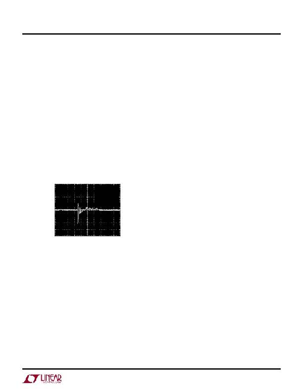
�4ms/DIV�
�capacitors,� but� can� still� be� significant� enough� to� drop�
�capacitor� values� below� appropriate� levels.� Capacitor� DC�
�bias� characteristics� tend� to� improve� as� component� case�
�size� increases,� but� expected� capacitance� at� operating�
�voltage� should� be� verified.�
�Voltage� and� temperature� coefficients� are� not� the� only�
�sources� of� problems.� Some� ceramic� capacitors� have� a�
�piezoelectric� response.� A� piezoelectric� device� generates�
�voltage� across� its� terminals� due� to� mechanical� stress,�
�similar� to� the� way� a� piezoelectric� accelerometer� or� mi-�
�crophone� works.� For� a� ceramic� capacitor,� the� stress� is�
�induced� by� vibrations� in� the� system� or� thermal� transients.�
�The� resulting� voltages� produced� cause� appreciable�
�amounts� of� noise.� A� ceramic� capacitor� produced� the� trace�
�in� Figure� 6� in� response� to� light� tapping� from� a� pencil.�
�Similar� vibration� induced� behavior� can� masquerade� as�
�increased� output� voltage� noise.�
�V� OUT� =� 0.6V�
�C� OUT� =� 10μF�
�C� REF/BYP� =� 10nF�
�I� LOAD� =� 100mA�
�V� OUT�
�500μV/DIV�
�3060� F06�
�Figure� 6.� Noise� Resulting� from� Tapping� on� a� Ceramic� Capacitor�
�Overload� Recovery�
�Like� many� IC� power� regulators,� the� LT3060� has� safe�
�operating� area� protection.� The� safe� operating� area� protec-�
�tion� decreases� current� limit� as� input-to-output� voltage�
�increases,� and� keeps� the� power� transistor� inside� a� safe�
�operating� region� for� all� values� of� input-to-output� voltage.�
�The� LT3060� provides� some� output� current� at� all� values� of�
�input-to-output� voltage� up� to� the� specified� 45V� operational�
�maximum.�
�When� power� is� first� applied,� the� input� voltage� rises� and� the�
�output� follows� the� input;� allowing� the� regulator� to� start-up�
�into� very� heavy� loads.� During� start-up,� as� the� input� voltage�
�is� rising,� the� input-to-output� voltage� differential� is� small,�
�allowing� the� regulator� to� supply� large� output� currents.�
�With� a� high� input� voltage,� a� problem� can� occur� wherein�
�the� removal� of� an� output� short� will� not� allow� the� output�
�to� recover.� Other� regulators,� such� as� the� LT1083/LT1084/�
�LT1085� family� and� LT1764A� also� exhibit� this� phenomenon,�
�so� it� is� not� unique� to� the� LT3060.� The� problem� occurs�
�with� a� heavy� output� load� when� the� input� voltage� is� high�
�and� the� output� voltage� is� low.� Common� situations� are:� (1)�
�immediately� after� the� removal� of� a� short-circuit� or� (2)� if�
�the� shutdown� pin� is� pulled� high� after� the� input� voltage� is�
�already� turned� on.� The� load� line� intersects� the� output� current�
�curve� at� two� points� creating� two� stable� output� operating�
�points� for� the� regulator.� With� this� double� intersection,� the�
�input� power� supply� needs� to� be� cycled� down� to� zero� and�
�brought� up� again� for� the� output� to� recover.�
�Thermal� Considerations�
�The� power� handling� capability� of� the� device� will� be� limited�
�by� the� maximum� rated� junction� temperature� (125°C� for�
�LT3060E,� LT3060I� or� 150°C� for� LT3060MP,� LT3060H).� Two�
�components� comprise� the� power� dissipated� by� the� device:�
�1.� Output� current� multiplied� by� the� input/output� voltage�
�differential:� I� OUT� ?� (V� IN� –V� OUT� ),� and�
�2.� GND� pin� current� multiplied� by� the� input� voltage:�
�I� GND� ?� V� IN�
�GND� pin� current� is� determined� using� the� GND� Pin� Current�
�curves� in� the� Typical� Performance� Characteristics� section.�
�Power� dissipation� equals� the� sum� of� the� two� components�
�listed� above.�
�The� LT3060� regulators� have� internal� thermal� limiting� that�
�protects� the� device� during� overload� conditions.� For� continu-�
�ous� normal� conditions,� the� maximum� junction� temperature�
�of� 125°C� (E-grade,� I-grade)� or� 150°C� (MP-grade,� H-grade)�
�must� not� be� exceeded.� Carefully� consider� all� sources� of�
�thermal� resistance� from� junction-to-ambient� including�
�other� heat� sources� mounted� in� proximity� to� the� LT3060.�
�The� underside� of� the� LT3060� DFN� package� has� exposed�
�metal� (1mm� 2� )� from� the� lead� frame� to� the� die� attachment.�
�The� package� allows� heat� to� directly� transfer� from� the� die�
�junction� to� the� printed� circuit� board� metal� to� control� maxi-�
�mum� operating� junction� temperature.� The� dual-in-line� pin�
�arrangement� allows� metal� to� extend� beyond� the� ends� of�
�3060fb�
�19�
�相关PDF资料 |
PDF描述 |
|---|---|
| FMC06DRYS-S734 | CONN EDGECARD 12POS DIP .100 SLD |
| FMC06DREI-S13 | CONN EDGECARD 12POS .100 EXTEND |
| ESC28DRYS-S734 | CONN EDGECARD 56POS DIP .100 SLD |
| LT3060IDC#TRMPBF | IC REG LDO ADJ .1A 8DFN |
| ESC25DRAN-S734 | CONN EDGECARD 50POS .100 R/A PCB |
相关代理商/技术参数 |
参数描述 |
|---|---|
| LT3060ITS8 | 制造商:LINER 制造商全称:Linear Technology 功能描述:45V VIN, Micropower, Low Noise, 100mA Low Dropout, Linear Regulator |
| LT3060ITS8#PBF | 制造商:Linear Technology 功能描述:LDO Regulator Pos 0.6V to 44.5V 0.1A 8-Pin TSOT-23 |
| LT3060ITS8#TRMPBF | 功能描述:IC REG LDO ADJ .1A 8TSOT RoHS:是 类别:集成电路 (IC) >> PMIC - 稳压器 - 线性 系列:- 产品培训模块:More Information on LDOs 标准包装:50 系列:- 稳压器拓扑结构:正,固定式 输出电压:3.3V 输入电压:最高 15V 电压 - 压降(标准):1.1V @ 800mA 稳压器数量:1 电流 - 输出:800mA 电流 - 限制(最小):800mA 工作温度:0°C ~ 125°C 安装类型:表面贴装 封装/外壳:TO-263-4,D²Pak(3 引线+接片),TO-263AA 供应商设备封装:D2PAK-3 包装:管件 |
| LT3060ITS8#TRPBF | 功能描述:IC REG LDO ADJ .1A 8TSOT RoHS:是 类别:集成电路 (IC) >> PMIC - 稳压器 - 线性 系列:- 产品培训模块:More Information on LDOs 标准包装:50 系列:- 稳压器拓扑结构:正,固定式 输出电压:3.3V 输入电压:最高 15V 电压 - 压降(标准):1.1V @ 800mA 稳压器数量:1 电流 - 输出:800mA 电流 - 限制(最小):800mA 工作温度:0°C ~ 125°C 安装类型:表面贴装 封装/外壳:TO-263-4,D²Pak(3 引线+接片),TO-263AA 供应商设备封装:D2PAK-3 包装:管件 |
| LT3060ITS8-1.2 | 制造商:LINER 制造商全称:Linear Technology 功能描述:45V VIN, Micropower, Low Noise, 100mA Low Dropout, Linear Regulator |
发布紧急采购,3分钟左右您将得到回复。