- 您现在的位置:买卖IC网 > PDF目录13087 > LT3085EDCB#TRMPBF (Linear Technology)IC REG LDO ADJ .5A 6-DFN PDF资料下载
参数资料
| 型号: | LT3085EDCB#TRMPBF |
| 厂商: | Linear Technology |
| 文件页数: | 14/28页 |
| 文件大小: | 0K |
| 描述: | IC REG LDO ADJ .5A 6-DFN |
| 产品培训模块: | LT3085 Adjustable Low Dropout Regulator More Information on LDOs |
| 标准包装: | 1 |
| 稳压器拓扑结构: | 正,可调式 |
| 输出电压: | 可调 |
| 输入电压: | 1.2 V ~ 36 V |
| 电压 - 压降(标准): | 1.35V @ 500mA |
| 稳压器数量: | 1 |
| 电流 - 输出: | 500mA |
| 电流 - 限制(最小): | 500mA |
| 工作温度: | -40°C ~ 125°C |
| 安装类型: | 表面贴装 |
| 封装/外壳: | 8-WFDFN 裸露焊盘 |
| 供应商设备封装: | 8-DFN-EP(3x3) |
| 包装: | 标准包装 |
| 产品目录页面: | 1331 (CN2011-ZH PDF) |
| 其它名称: | LT3085EDCB#TRMPBFDKR |
第1页第2页第3页第4页第5页第6页第7页第8页第9页第10页第11页第12页第13页当前第14页第15页第16页第17页第18页第19页第20页第21页第22页第23页第24页第25页第26页第27页第28页
�� �
�
�LT3085�
�APPLICATIONS� INFORMATION�
�The� problem� occurs� with� a� heavy� output� load� when� the�
�input� voltage� is� high� and� the� output� voltage� is� low.� Com-�
�mon� situations� are� immediately� after� the� removal� of� a�
�short� circuit.� The� load� line� for� such� a� load� may� intersect�
�the� output� current� curve� at� two� points.� If� this� happens,�
�there� are� two� stable� operating� points� for� the� regulator.�
�With� this� double� intersection,� the� input� power� supply� may�
�need� to� be� cycled� down� to� zero� and� brought� up� again� to�
�make� the� output� recover.�
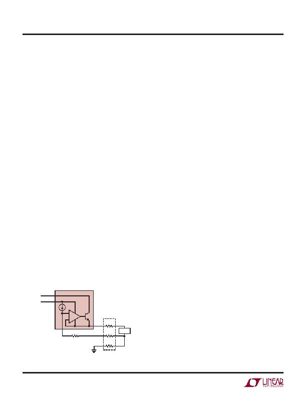
�Load� Regulation�
�Because� the� LT3085� is� a� ?oating� device� (there� is� no� ground�
�pin� on� the� part,� all� quiescent� and� drive� current� is� delivered�
�to� the� load),� it� is� not� possible� to� provide� true� remote� load�
�sensing.� Load� regulation� will� be� limited� by� the� resistance�
�of� the� connections� between� the� regulator� and� the� load.�
�The� data� sheet� speci?cation� for� load� regulation� is� Kelvin�
�sensed� at� the� pins� of� the� package.� Negative� side� sensing�
�is� a� true� Kelvin� connection,� with� the� bottom� of� the� voltage�
�setting� resistor� returned� to� the� negative� side� of� the� load�
�(see� Figure� 7).� Connected� as� shown,� system� load� regulation�
�will� be� the� sum� of� the� LT3085� load� regulation� and� the�
�parasitic� line� resistance� multiplied� by� the� output� current.�
�It� is� important� to� keep� the� positive� connection� between�
�the� regulator� and� load� as� short� as� possible� and� use� large�
�wire� or� PC� board� traces.�
�Internal� Parasitic� Diodes� and� Protection� Diodes�
�In� normal� operation,� the� LT3085� does� not� require� protection�
�diodes.� Older� three-terminal� regulators� require� protection�
�diodes� between� the� VOUT� pin� and� the� input� pin� or� between�
�the� ADJ� pin� and� the� VOUT� pin� to� prevent� die� overstress.�
�On� the� LT3085,� internal� resistors� and� diodes� limit� current�
�paths� on� the� SET� pin.� Even� with� bypass� capacitors� on� the�
�SET� pin,� no� protection� diode� is� needed� to� ensure� device�
�safety� under� short-circuit� conditions.� The� SET� pin� handles�
�±10V� (either� transient� or� DC)� with� respect� to� OUT� without�
�any� device� degradation.�
�Internal� parasitic� diodes� exist� between� OUT� and� the� two�
�inputs.� Negative� input� voltages� are� transferred� to� the� output�
�and� may� damage� sensitive� loads.� Reverse-biasing� either�
�input� to� OUT� will� turn� on� these� parasitic� diodes� and� allow�
�current� ?ow.� This� current� ?ow� will� bias� internal� nodes�
�of� the� LT3085� to� levels� that� possibly� cause� errors� when�
�suddenly� returning� to� normal� operating� conditions� and�
�expecting� the� device� to� start� and� operate.� Prediction� of�
�results� of� a� bias� fault� is� impossible,� immediate� return� to�
�normal� operating� conditions� can� be� just� as� dif?cult� after�
�a� bias� fault.� Suf?ce� it� to� say� that� extra� wait� time,� power�
�cycling,� or� protection� diodes� may� be� needed� to� allow� the�
�LT3085� to� return� to� a� normal� operating� mode� as� quickly�
�as� possible.�
�Protection� diodes� are� not� otherwise� needed� between�
�the� OUT� pin� and� IN� pin.� The� internal� diodes� can� handle�
�microsecond� surge� currents� of� up� to� 50A.� Even� with�
�large� output� capacitors,� obtaining� surge� currents� of� those�
�magnitudes� is� dif?cult� in� normal� operation.� Only� with� large�
�output� capacitors,� such� as� 1000μF� to� 5000μF,� and� with�
�IN� instantaneously� shorted� to� ground� will� damage� occur.�
�A� crowbar� circuit� at� IN� is� capable� of� generating� those�
�levels� of� currents,� and� then� protection� diodes� from� OUT�
�to� IN� are� recommended.� Normal� power� supply� cycling� or�
�system� “hot� plugging� and� unplugging”� does� not� do� any�
�damage.�
�IN�
�V� CONTROL�
�LT3085�
�A� protection� diode� between� OUT� and� V� CONTROL� is� usually�
�not� needed.� The� internal� parasitic� diode� on� V� CONTROL� of�
�the� LT3085� handles� microsecond� surge� currents� of� 1A� to�
�+�
�–�
�OUT�
�PARASITIC�
�RESISTANCE�
�R� P�
�10A.� Again,� this� only� occurs� when� using� crowbar� circuits�
�with� large� value� output� capacitors.� Since� the� V� CONTROL�
�pin� is� usually� a� low� current� supply,� this� is� unlikely.� Still,�
�SET� R� SET�
�R� P�
�R� P�
�LOAD�
�3085� F07�
�a� protection� diode� is� recommended� if� V� CONTROL� can� be�
�instantaneously� shorted� to� ground.� Normal� power� supply�
�cycling� or� system� “hot� plugging� and� unplugging”� does�
�not� do� any� damage.�
�Figure� 7.� Connections� for� Best� Load� Regulation�
�3085fb�
�14�
�相关PDF资料 |
PDF描述 |
|---|---|
| HBC50DRTH-S13 | CONN EDGECARD 100PS .100 EXTEND |
| RBA44DCBT | CONN EDGECARD 88POS R/A .125 SLD |
| RBB25DHBT | CONN EDGECARD 50POS R/A .050 DIP |
| 420VXG150MEFCSN25X30 | CAP ALUM 150UF 420V 20% SNAP-IN |
| C1005X7R1E103K | CAP CER 10000PF 25V 10% X7R 0402 |
相关代理商/技术参数 |
参数描述 |
|---|---|
| LT3085EDCB-TRPBF | 制造商:LINER 制造商全称:Linear Technology 功能描述:Adjustable 500mA Single Resistor Low Dropout Regulator |
| LT3085EMS8E | 制造商:Linear Technology 功能描述:LDO Regulator Pos 0V to 36V 0.5A 8-Pin MSOP EP |
| LT3085EMS8E#PBF | 功能描述:IC REG LDO ADJ .5A 8-MSOP RoHS:是 类别:集成电路 (IC) >> PMIC - 稳压器 - 线性 系列:- 产品培训模块:MIC5365/66 Ultra-small LDO Regulators 标准包装:1 系列:- 稳压器拓扑结构:正,固定式 输出电压:3V 输入电压:最高 5.5V 电压 - 压降(标准):0.155V @ 150mA 稳压器数量:1 电流 - 输出:150mA 电流 - 限制(最小):200mA 工作温度:-40°C ~ 125°C 安装类型:表面贴装 封装/外壳:4-UDFN 裸露焊盘,4-TMLF? 供应商设备封装:4-TMLF?(1x1) 包装:Digi-Reel® 其它名称:576-3192-6 |
| LT3085EMS8E#TRPBF | 功能描述:IC REG LDO ADJ .5A 8-MSOP RoHS:是 类别:集成电路 (IC) >> PMIC - 稳压器 - 线性 系列:- 标准包装:800 系列:- 稳压器拓扑结构:正,固定式 输出电压:2.5V 输入电压:最高 16V 电压 - 压降(标准):0.7V @ 4A 稳压器数量:1 电流 - 输出:4A 电流 - 限制(最小):4.2A 工作温度:0°C ~ 125°C 安装类型:表面贴装 封装/外壳:TO-263-6,D²Pak(5 引线+接片),TO-263BA 供应商设备封装:TO-263-5 包装:带卷 (TR) 其它名称:AP1184K525L-13AP1184K525LDITR |
| LT3085EMS8EPBF | 制造商:Linear Technology 功能描述:LDO Regulator Adj. 0.5A Resistor MSOP8EP |
发布紧急采购,3分钟左右您将得到回复。